Is the ASUS Xonar H6 2x12pin header specification available ? PCIe 1x only used for DC supply ?
I'll post the pinout when I get home tonight, guess its ok. There is no PCIe connector actually, the card edge looking like it is just used to mount the board, supply is via the header only.
I think we talked about this around post 365, though not specifically about connector pinouts. ADCs, DACs, codecs, and SPDIF receivers are all I2S sources and sinks, so in all cases I'm aware of board to board interfaces among these and a DSP are I2S into the DSP and I2S out of the DSP. There's kind of a de facto standard of using 100 mil headers for the interconnect to the DSP, though I'm not aware of any case where boards from different manufacturers assign the same I2S lines to the same pins on the header (or even use headers with the same number of pins, now that I think about it).Now has anyone designed his/her own boards yet?
So, to do what you're proposing, one ends up either building custom ribbon cables for the combinations of interest or building adapter boards to do the same thing. This is no big deal, but it does mean any pinout standard one defines is going to be "wrong" most of the time, unless it happens to take off and become widely supported. To my mind the most interesting pinouts are in the 4x8 space---two I2S lines into the DSP to support switching between a couple sources and four lines out to support four ways---but 2x2, 2x4, 2x6, 2x8, 4x2, 4x4, 4x6, 4x8, and 8x8 are all fairly common (and those are just the variations I can think of people on DIYA using off the top of my head).
Having extra IOs that are unused is better than not exposing IOs that are needed so targeting (more)x(more) seems the preferred default. The LPC4300 has the I2S peripherals and SGPIO slices for two 4x8 interfaces (though I'm not sure about doing both at the same time with independent clocks). It's also useful to pin out I2C, some GPIOs for things like reset, and maybe power and an ADC for a volume pot.
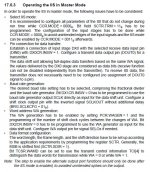
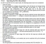
Back when I looked at the part I saw no problem generating the LRCK. But I didn't look all that closely.I'm not sure if XMC4500 can generate the LRCLK in slave mode
Here's the pinout of H6 board. The numbering starts from pin 1 of J1 connector but is kind of odd. The pins are numbered from left up pin 1 to left down pin 13 and then the right pins from pin 14 to pin 26 (like opams are numbered):
Some not connected pins may be conected to ground or should be connected to ground for the sound card to recognize that H6 is present, but it doesn't matter (hopefully) when used standalone.
Code:
[SIZE="2"][SIZE="1"][FONT="Courier New"]======= XONAR HDAV H6 pinout ================
                                      V
 13 12 11 10 09 08 07 06 05 04 03 02 01
(26)25 24 23 22 21 20 19 18 17 16 15 14

01) RST (pcm1796)
02) MDI (pcm1796 right dac), /MS (pcm1796 middle dac), GND
03)
04) GND
05) RELAY ON
06) MDO (pcm1796) = I2C DATA
07) MC (pcm1796) = I2C CLOCK
08) VDD (digital supply 3.3V)
09) VCC  (analog supply 5V)
10) analog/digital ground
11) op amp +ve (+15V)
12)
13) op amp -ve (-15V)

14)
15)
16) MDI (pcm1796 right dac), /MS (pcm1796 middle dac), GND
17) DATA (pcm1796 middle dac)
18) DATA (pcm1796 left dac)
19) DATA (pcm1796 right dac)
20)
21) LRCK (pcm1796)
22) BCK (pcm1796)
23) SCK (pcm1796)
24) GND
25)
26) missing pin

I2C slave addresses
====================

PCM1796 left dac:  /MC=1 (=ADR0),  MDI=1 (=ADR1) => 1001111
PCM1796 middle dac: /MS=0, MDI=1 => 1001110
PCM1796 right dac: /MS=1, MDI=0 => 1001101
[/FONT][/SIZE][/SIZE]
Some not connected pins may be conected to ground or should be connected to ground for the sound card to recognize that H6 is present, but it doesn't matter (hopefully) when used standalone.
Last edited:
I'm using a mix of the 4300's I2S and SGPIO peripherals and the preliminary schematic includes an expansion header with duplex clocking, I2S receive, and the seven SGPIO lines that aren't used for driving the 4365.
So it's not modular per se, but if one wants to patch in an ADC, different multichannel DAC, alternate clock, or pretty much any arbitrary I2S source or sink it's not particularly difficult.
Haven't been able to find an LPC4300 evaluation board with the I2S and SGPIO pins exposed to headers, aren't there really any? The latest Embest/Element14 LPC4357 (builtin flash part) boards either have those pins (they are missing all SGIOP pins too, don't know what they have been thinking when designing those boards). Can't the SGPIO used full duplex? Anyway, there is a new LPC4357 board coming from NGX Tech:
NGX Technologies Online Store
It doesn't need external flash but there is still one chip on board. I think if I remove the flash chip I could take the second I2S port pins from there. Might be difficult depending on package (SOIC should be possible to handle).
Btw. STM32F4 has two I2S outputs (has been discussed earlier). However, these are mapped (so to say) to SPI2 and SPI3 (which are working in I2S mode). This leaves SPI1 free, and if I2S LRCLK could be converted to SPI frame syncs happening excactly 16 bits (SCLK's) apart it would be possible with the help of DMA to output data for additional I2S channels 5/6.
The SPI frame is max. 16 bit but in continuous TI SPI mode you just output continuosly data so that it will be eventually output to DAC in correct I2S frame. Don't know what happens if the synchronization with I2S block (interrupts) breaks, anyway if the are started together and synchronized by LRCLK and SCLK there shouldn't be problems. Kind of hack though, but by using DMA it might actually work. One problem is that the SPI sync (NSS pin) occurs during last bit output, so that's one sample before I2S LRCLK transition occurs. However, because in I2S the first bit (MSB) is anyway delayed by one clock it goes as it should. Problem is generating the NSS 16 clocks later (use some counter or flip-flops, not many chips are needed I guess).
The SPI frame is max. 16 bit but in continuous TI SPI mode you just output continuosly data so that it will be eventually output to DAC in correct I2S frame. Don't know what happens if the synchronization with I2S block (interrupts) breaks, anyway if the are started together and synchronized by LRCLK and SCLK there shouldn't be problems. Kind of hack though, but by using DMA it might actually work. One problem is that the SPI sync (NSS pin) occurs during last bit output, so that's one sample before I2S LRCLK transition occurs. However, because in I2S the first bit (MSB) is anyway delayed by one clock it goes as it should. Problem is generating the NSS 16 clocks later (use some counter or flip-flops, not many chips are needed I guess).
I haven't particularly looked as the BOM cost to solder down an LPC4300 on one of my own boards is comparable to or less than most of the eval boards. Not that I expect to run boards any time soon; still have to get the firmware together and haven't settled on how I want the DSP+DAC board to fit in with its power supply and low/mid power amplifier I want to put in the same chassis.Haven't been able to find an LPC4300 evaluation board with the I2S and SGPIO pins exposed to headers, aren't there really any?
Thanks for pointing it, just bought a few from Mouser.The Infineon XMC4500 Relax Lite kit (which also includes USB debugger) costs only 12.95 EUR on Mouser
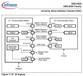
I went digging the XMC4500 Datasheet and XMC4500 Reference Manual, trying to figure what the advertised "6 x I2S" really means :
USIC#0 : U0.C0 (channel 0) and U0.C1 (channel 1)
USIC#1 : U1.C0 (channel 0) and U1.C1 (channel 1)
USIC#2 : U2.C0 (channel 0) and U2.C1 (channel 1)
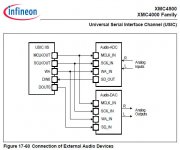
For connecting a WM8580 containing two ADCs and six DACs, the following lines are needed (viewed from the XMC4500) :
- I2S_data_in1
- I2S_data_out1
- I2S_data_out2
- I2S_data_out3
- I2S_SCLK
- I2S_WS
- I2C_SCL (as control bus)
- I2C_SDA (as control bus)
Can somebody advise me how to assign the USICs on the Infineon XMC4500 Relax Lite kit ?
If such assignment is feasible, I will stop developing for the PIC32MX2, and join the ARM Cortex-M4 bandwagon.
Attachments
-
 XMC4500 USIC I2S in Master Mode.jpg214.1 KB · Views: 208
 -
 XMC4500 USIC I2S in Slave Mode.jpg168.6 KB · Views: 208
 -
 XMC4500 USIC I2S Connecting Audio Devices.jpg60.3 KB · Views: 199
 -
 XMC4500 USIC I2S Signals.jpg79.2 KB · Views: 203
 -
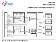 XMC4500 USIC Data Buffering.jpg122.4 KB · Views: 185
 -
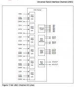 XMC4500 USIC Channel IO Lines.jpg70.7 KB · Views: 52
Last edited:
The Relax kit board user manual (Infineon Technologies ) shows in figure 6 example of the pin mappings though it is missing data inputs pins. You have to download the XMC4500 Reference Manual and look for the needed pins and deside the mapping you will use (there are usually several alternatives). Manual can be found here:
Infineon Technologies
Unfortunately I wasn't able to find any code examples. Easiest approach would be using DAVE 3 tool, but it seems that I2S application is not yet ready. Basically you has to decide which clocking schemes are available and what you will use (master/slave), set all needed registers for generating the proper clock, setup the DMA and interrupt(s), word and frame size for I2S block and then enable the clock and I2S blocks. Guess DAVE SPI application could be used for setting up DMA and interrupts at least.
Reading more than 100 pages, I still don't know what the advertised "6 x I2S" really means. At the moment, I don't care about the pin mapping. At the moment I need to know what the advertised "6 x I2S" really means. I'm not going to invest time, dealing with pin mapping, before I understand the advertised "6 x I2S". Currently, as you wrote, the Relax kit board user manual (Infineon Technologies ) shows in figure 6 example of the pin mappings though it is missing data inputs pins. Currently, DAVE is not able to setup the USICs as I2S. There must be a catch somewhere.I went digging the XMC4500 Datasheet and XMC4500 Reference Manual, trying to figure what the advertised "6 x I2S" really means.
For connecting a WM8580 containing two ADCs and six DACs, the following lines are needed (viewed from the XMC4500) :
- I2S_data_in1
- I2S_data_out1
- I2S_data_out2
- I2S_data_out3
- I2S_SCLK
- I2S_WS
- I2C_SCL (as control bus)
- I2C_SDA (as control bus)
Can somebody advise me how to assign the USICs on the Infineon XMC4500 Relax Lite kit ?
Can somebody advise me how to assign the USICs on the Infineon XMC4500 Relax Lite kit ?
Sorry, don't understand what you mean with "assign the USICs". Anyway, each of six USIC channels, two per each independent USIC (3x2=6) have independent address space, see 17.11.1 Address Map
Table 17-20 Registers Address Space
Module Base Address End Address
---------------- ---------------- ---------------
USIC0_CH0 40030000H 400301FFH
USIC0_CH1 40030200H 400303FFH
USIC1_CH0 48020000H 480201FFH
USIC1_CH1 48020200H 480203FFH
USIC2_CH0 48024000H 480241FFH
USIC2_CH1 48024200H 480243FFH
So you can connect your I2S_data_in to for an example USIC0_CH0.DX0A input, or any of these:
Table 17-22 USIC Module 0 Channel 0 Interconnects
Input/Output
I/O Connected To Description
USIC0_CH0.DX0A I P1.5 Shift data input
USIC0_CH0.DX0B I P1.4 Shift data input
USIC0_CH0.DX0C I P4.7 Shift data input
USIC0_CH0.DX0D I P5.0 Shift data input
(there are more input "pins" like loopback and XTAL but not very useful)
Likewise output goes to output USIC0_CH0.DOUT0 (multiple locations), or generally to USICn_CHy.DOUT0 where n=0,1,2 and y=0,1.
@mhelin, thanks a zillion for helping me!
What do you think about the following pin multiplexing approaches?
- ALT2 looks nice for four bidirectional I2S, featuring all control signals, however I don't know if I2C and SPI can be added (for the WM8580, one I2C is needed).
- Within the ALT2 scheme, is it allowed to configure U1C1 as I2C instead of I2S? This way there are three I2S and one I2C.
- HWO0 looks nice for six communication channels, however all control signals seem to be missing, and we need them. How to add them?
Is is allowed to blend "ALT2" and "HWO0" perhaps ?
*****************************************************
XMC4500 : ALT2 = four I2S_out plus four I2S_in with all control signals
*****************************************************
U0C0
****
DOUT0 P1.5 I2S out
DX0B P1.4 I2S in
SEL0 P1.0 Frame Sync
SCLK P1.1 Shift Clock
MCLK P1.2 High Frequency Clock (not needed with WM8580 or WM8581)
U0C1
****
DOUT0 P3.13 I2S out
DX0D P3.12 I2S in (not needed with WM8580 or WM8581)
SEL0 P6.1 Frame Sync
SCLK P6.2 Shift Clock
MCLK P6.5 High Frequency Clock (not needed with WM8580 or WM8581)
U1C0
****
DOUT0 P0.5 I2S out
DX0A P0.4 I2S in (not needed with WM8580 or WM8581)
SEL0 P5.9 Frame Sync
SCLK P5.8 Shift Clock
MCLK P5.10 High Frequency Clock (not needed with WM8580 or WM8581)
U1C1
****
DOUT0 P0.1 I2S out (only with WM8581)
DX0D P0.0 I2S in (not needed with WM8580 or WM8581)
SEL0 P0.9 Frame Sync
SCLK P0.10 Shift Clock
MCLK P4.1 High Frequency Clock (not needed with WM8580 or WM8581)
U2C0
****
Question : is it available as I2C (dedicated WM8580/WM8581 control bus) ?
U2C1
****
Question : is it available as SPI (general control bus) ?
*******************************************************
XMC4500: HWO0 = six I2S_out plus six I2S_in without any control signal
*******************************************************
U0C0
****
DOUT0 P1.5 I2S out
DX0B P1.4 I2S in
U0C1
****
DOUT0 P3.13 I2S out
DX0D P3.12 I2S in (not needed with WM8580 or WM8581)
U1C0
****
DOUT0 P0.5 I2S out
DX0A P0.4 I2S in (not needed with WM8580 or WM8581)
U1C1
****
DOUT0 P3.15 I2S out
DX0B P3.14 I2S in (not needed with WM8580 or WM8581)
U2C0
****
DOUT0 P5.0 Ideally, this would be a I2C bus (as dedicated WM8580/WM8581 control bus)
DX0A P5.1
U2C1
****
DOUT0 P4.7 Ideally, this would be a SPI (as general control bus)
DX0A P3.5 (consumes SDMMC.CMD_OUT)
Question : for all six serial interfaces, how to get the control signals SEL0 and SCLK ?
Infineon is advertising "6 x I2S".
Do they mean "6 x full duplex I2S" ?
Configuring all USICs as I2S, is it possible to sync all six I2S on a common Frame_Sync and Shift_Clock ?
Last edited:
I haven't studied output pinning but I think you can select mode for each pin separately. I would prefer ALT modes because I2S doesn't need HW modes (don't know which interface or protocol requires them but some will). Input pinning, well it's quite free. Regarding the channel protocols you control them via CCR.MODE register, thats Channel Control Register, so I assume you can select different protocol for each channel if needed:
------
CCR
MODE [3:0] rw Operating Mode
This bit field selects the protocol for this USIC
channel. Selecting a protocol that is not available (see
register CCFG) or a reserved combination disables
the USIC channel. When switching between two
protocols, the USIC channel has to be disabled
before selecting a new protocol. In this case, registers
PCR and PSR have to be cleared or updated by
software.
0H The USIC channel is disabled. All protocolrelated
state machines are set to an idle state.
1H The SSC (SPI) protocol is selected.
2H The ASC (SCI, UART) protocol is selected.
3H The IIS protocol is selected.
4H The IIC protocol is selected.
Other bit combinations are reserved.
---
It's good idea to think which serial protocols are needed first. I2C or SPI for DAC/CODEC control, yes. Then how about UART, do you want to update the biquads using simple UART terminal? How about USB, could it be used for downloading filter coefficients? Does USB need isolator to avoid ground loops (off topic but good question if you are planning to use USB)?
If one I2S is master then other I2S channels can be slaves and for sure can be synched (though may need external links). There may be other ways but I'm not sure. I haven't ordered those kits yet because I'd like order them from Mouser with other stuff to fullfil the 65 EUR limit to get free delivery at least (must pay the VAT unfortunately here in Europe). LPC4300 looks better because of the speed and SGPIO, though there may be some hidden things preventing good performance. For an example the XMC4500 does have internal cache which is excellent thing at high clock speeds. I don't know if anyone has tried overclocking them yet (if that's possible), but at least the performance wouldn't be lacking because of the need to use wait states to read program code or data from slow flash. Anyway the XMC part looks good, it seems to be better for xover application than STM32F4 because of the USIC's. The DAVE might make programming easier when it gets I2S support - it might be good idea to download the software and try to use it if not for I2S then for I2C or SPI, it might be the generated code is easy to change to use I2S protocol by changing just the CCR.MODE setting and pinning.
Then there are at least two ways to handle the I/O buffering - either use FIFO or DMA. FIFO is simpler to start, but it's difficult to evaluate the performance. Maybe you can enable some GPIO pins and output some strobes and look with oscilloscope how long the subroutine takes time.
This pdf mentions XMC4700 chip with 180 MHz clock, 512kB RAM, 2Mb flash and 6 kB cache:
http://www.hardwareconference.nl/fi...hw/2012/Sprekers/Presentaties/Ingo_Skuras.pdf
Now that would be something, hopefully there will be new Relax Lite kit with that chip (it might be possible they are pin-compatible).
E: The XMC4700 is out Q1 2014 so no reason to wait for it now.
http://www.hardwareconference.nl/fi...hw/2012/Sprekers/Presentaties/Ingo_Skuras.pdf
Now that would be something, hopefully there will be new Relax Lite kit with that chip (it might be possible they are pin-compatible).
E: The XMC4700 is out Q1 2014 so no reason to wait for it now.
Last edited:
XMC4500 : is this feasible?
4 x bidirectional I2S with the XMC4500 as slave connecting to a WM8580 or WM8581 codec
1 x bidirectional SPI with four chip_select
1 x I2C
I'm suggesting :
P0.0 U1C1.I2S_data_in (DX0D)
P0.1 U1C1.I2S_data_out (DOUT0) in ALT2
P0.9 U1C1.I2S_frame_sync_in (DX2A)
P0.10 U1C1.I2S_sclk_in (DX1A)
P0.4 U1C0.I2S_data_in (DX0A)
P0.5 U1C0.I2S_data_out (DOUT0) in ALT2 or HWO0
P0.6 U1C0.I2S_frame_sync_in (DX2A)
P0.11 U1C0.I2S_sclk_in (DX1A)
P1.0 U0C0.I2S_frame_sync_in (DX2A)
P1.1 U0C0.I2S_sclk_in (DX1A)
P1.4 U0C0.I2S_data_in (DX0B)
P1.5 U0C0.I2S_data_out (DOUT0) in ALT2 or HWO0
P2.2 U0C1.I2S_data_in (DX0A)
P2.3 U0C1.I2S_frame_sync_in (DX2A)
P2.4 U0C1.I2S_sclk_in DX1A)
P2.5 U0C1.I2S_data_out (DOUT0) in ALT2
P3.4 ?
P3.5 U2C1.I2C_sda (DOUT0) in ALT1
P3.6 U2C1.I2C_scl (SCLKOUT) in ALT1
P5.0 U2C0.SPI_data_out (DOUT0) in ALT1
P5.1 U2C0.SPI_data_in (DX0A)
P5.2 U2C0.SPI_sclk_out (SCLKOUT) in ALT1
P5.3 U2C0.SPI_sel0_out (SEL0) in ALT1
P5.4 U2C0.SPI_sel1_out (SEL1) in ALT1
P5.5 U2C0.SPI_sel2_out (SEL2) in ALT1
P5.6 U2C0.SPI_sel3_out (SEL3) in ALT1
Within the I2S domain, all sclk_in connecting together.
Within the I2S domain, all frame_sync_in connecting together.
All this, plus USB for updating the filters coefficients.
Configuring U0C1 as UART instead of I2S during development for updating the filters coefficients, in case USB is not working yet.
Thanks for helping.
Last edited:
XMC4500 Relax Lite Kit-V1: is this feasible?
3 x bidirectional I2S with the XMC4500 as slave connecting to a WM8580 or WM8581 codec
1 x bidirectional SPI or I2C
I'm suggesting :
P0.0 U1C1.I2S_data_in (DX0D) @ pin 32 header X1
P0.1 U1C1.I2S_data_out (DOUT0) in ALT2 @ pin 34 header X1
P0.9 U1C1.I2S_frame_sync_in (DX2A) @ pin 33 header X1
P0.10 U1C1.I2S_sclk_in (DX1A) @ pin 35 header X1
P0.4 U1C0.I2S_data_in (DX0A) @ pin 34 header X2 (not really needed)
P0.5 U1C0.I2S_data_out (DOUT0) in ALT2 or HWO0 @ pin 31 header X2
P0.6 U1C0.I2S_frame_sync_in (DX2A) @ pin 30 header X2
P0.11 U1C0.I2S_sclk_in (DX1A) @ pin 29 header X2
P1.0 U0C0.I2S_frame_sync_in (DX2A) @ pin 21 header X2
P1.1 U0C0.I2S_sclk_in (DX1A) @ pin 20 header X2
P1.4 U0C0.I2S_data_in (DX0B) @ pin 17 header X2 (not really needed)
P1.5 U0C0.I2S_data_out (DOUT0) in ALT2 or HWO0 @ pin 16 header X2
P5.0 U2C0.SPI_data_out or U2C0.I2C_sda (DOUT0) or in ALT1 @ pin 9 header X2
P5.1 U2C0.SPI_data_in (DX0A) @ pin 8 header X2
P5.2 U2C0.SPI_sclk_out or U2C0.I2C_scl (SCLKOUT) in ALT1 @ pin 7 header X2
Within the I2S domain, all sclk_in connecting together.
Within the I2S domain, all frame_sync_in connecting together.
All this, plus USB for updating the filters coefficients.
Thanks for helping.
Last edited:
Looks go to me, good plan for testing at least. I2S pins are grouped nicely closely together. Just build a breadboardable WM8580 board (with single row headers) first and try those combos.
Btw. This presentation claims that DAVE 3 supports among other Peripherals Specific Apps USIC (I2S, I2C, UART, SPI).
http://www.infineon.com/dgdl/DAVE-3...f0281&fileId=db3a304335c2937a0135e35a63974506
Btw. This presentation claims that DAVE 3 supports among other Peripherals Specific Apps USIC (I2S, I2C, UART, SPI).
http://www.infineon.com/dgdl/DAVE-3...f0281&fileId=db3a304335c2937a0135e35a63974506
Btw. This presentation claims that DAVE 3 supports among other Peripherals Specific Apps USIC (I2S, I2C, UART, SPI).
http://www.infineon.com/dgdl/DAVE-3...f0281&fileId=db3a304335c2937a0135e35a63974506
Installed DAVE and downloaded the application libraries (through some Eclipse menu). The I2S application was now listed there among applications, and I was able to create a full-duplex I2S application with DMA support. Only drawback was that only 16-bit word size was supported. Got to ask Infineon why. I don't have the board so wasn't able to test. It seems CMSIS-RT OS (RTX) comes in with the build, and you have only limited support what features to disable. The generated I2S F/D DMA app used OS Semaphores at least. The generated code looks reasonable, I think you need just call some I2S002_Start() function and after that some getNextRxDMABuffer() or something, process data and store it to next Tx DMA buffers (I think) for playback.
In DAVE GUI there are also menus for manual pinning, that's nice feature.
Bad news, XMC4500 is supporting only 16-bit word length :
-------
SCTR
Shift Control Register
WLE [27:24] rwh Word Length
This bit field defines the data word length (amount of
bits that are transferred in each data word) for
reception and transmission. The data word is always
right-aligned in the data buffer at the bit positions
[WLE down to 0].
If TCSR.WLEMD = 1, the value can be updated
automatically by the data handler.
The data word contains 1 data bit located at bit
0H
position 0.
The data word contains 2 data bits located at bit
1H
positions [1:0].
...
The data word contains 15 data bits located at
EH
bit positions [14:0].
The data word contains 16 data bits located at
FH
bit positions [15:0].
Reference Manual
USIC, V2.10
17-184
V1.2, 2012-12
Subject to Agreement on the Use of Product Information
--------
Too bad they reserved only four bits for data word length register, wrong place to save bits.
Last edited:
Bad news, XMC4500 is supporting only 16-bit word length
WLE [27:24] rwh Word Length
This bit field defines the data word length (amount of bits that are transferred in each data word) for reception and transmission. The data word is always right-aligned in the data buffer at the bit positions [WLE down to 0]. If TCSR.WLEMD = 1, the value can be updated automatically by the data handler.
0H The data word contains 1 data bit located at bit position 0.
1H The data word contains 2 data bits located at bit positions [1:0].
...
EH The data word contains 15 data bits located at bit positions [14:0].
FH The data word contains 16 data bits located a bit positions [15:0].
Reference Manual
USIC, V2.10
17-184
V1.2, 2012-12
Subject to Agreement on the Use of Product Information
Ok, if you listen to redbook audio mostly then 16-bit I2S data (in/out) is ok, this doesn't limit processing anyway. At least it's fine if you have analog volume controller after DAC(s). In any case your total DR will be more that that of 16-bit system because you have multiple 16-bit DACs summed in actual speakers.
- Status
- This old topic is closed. If you want to reopen this topic, contact a moderator using the "Report Post" button.
- Home
- Source & Line
- Digital Line Level
- Open Source DSP XOs