This project sounds extremely interesting, congrats for taking on such a beautiful design.
However, I believe that it should be discussed in a separate thread because this thread is talking about a simple ARM-based design, and I suggest that you guys post a link to your thread and allow the OP to develop here his idea.
Kindest greetings,
Nick
(Link posted in previous post, apologies)
However, I believe that it should be discussed in a separate thread because this thread is talking about a simple ARM-based design, and I suggest that you guys post a link to your thread and allow the OP to develop here his idea.
Kindest greetings,
Nick
(Link posted in previous post, apologies)
Last edited:
Whatever floats your boat for linux development. The board will run a wide variety of OS. I am currently booting Ubuntu or Gingerbread on the EVM. Have you come across the BeagleBoard before? I'm building a more powerful version of that.
Yes I have seen the beagle board but it hasn't got much in the way of on-board audio.
regards
Trev
Consider the discussion moved.")
Thanks
Good luck with your project!@chaparK - thanks for your support for keeping this thread on-topic
16 slices, max SGPIO_CLOCK of 204MHz.* In theory that's 14 32 bit I2S lines at 1.536MHz---enough to operate 3.5 eight channel ESS DACs at their maximum input rate---though one would likely run out of CPU first and one would probably want more than one BLCK and LRCLK. A more typical upper bound for a DSP XO would be three or four I2S at 352.8kHz. This allows use of the 8Fs bypass mode in DACs which have it, meaning the lowpasses in the crossover can be provide some or all of the antialiasing filtering. Things get tricky with the tweeter but basically one gets something which combines the low THD, high SNR, and ready parts availability of sigma-delta DACs with time domain behavior which begins to approximate that of a NOS DAC.The SGPIO looks very useful, and I think he said there are 8 on the chip, so that's potentially 16 stereo DAC chips or even more channels if you're willing to use multichannel chips (assuming the clock rates of the SGPIO can keep up).
Whether or not this would have audible effects is debatable but I have reason to suspect that, when combined with other sources of preringing such as linear phase crossovers, there's likely some advantage to reducing DAC preringing. So it would be interesting to give it a try and find out. From what I'm seeing the LPC43x0 is probably the lowest cost DSC or DSP based way to do this and hence the best suited for DIY. Parts with IO capabilities comparable to SGPIO aren't necessarily a whole lot more expensive but the cost risers for development environments and programmer/debuggers all seem to be significant compared to LPCxpresso and a Red Probe. There might be a viable FPGA alternative---at this point I haven't looked.
In this presentation there's biquad performance data at 25:30 which works out to just under 100% CPU utilization on the LPC4300's M4 core with 37 stereo biquads at 44.1. It’s unclear if the biquads in question are 16 bit fixed point, 32 bit fixed point, single precision floating point, or double precision. My guess is floating point, as the last presentation here indicates 47 32 bit stereo biquads at 44.1. My three way crossover and EQ is probably a little more complex than most and totals 23 biquads. That implies a single LPC4300 solution should work well for most CD audio processing needs and could accommodate 24/96 from DVD. Unfortunately I would like to operate at least 9 biquads at 8Fs and just those 9 want 175% of a 180MHz M4 core. That suggests one LPC4300 for the tweeters, another for the midrange, and a third for the subs.
Perhaps a clever algorithm can be found but, given the feedback in IIR filters, I’m not immediately seeing one. (There is a special case where, if oversampling is implemented by zero stuffing, one could do some loop unrolling and take advantage of the zeros to operate an oversampled biquad at roughly the same cycle count as a biquad at Fs. Only works for the first biquad in the oversampled filter chain, though.)DigiKey has one one LPC4300 part in stock so far and it's a BGA. Pricing is attractive, though. The parts cost for three LPC4300s is roughly equal to a Blackfin with comparable processing power. A little more soldering but no several thousand dollar Visual DSP license.
* Not counting the two dedicated I2S peripherals.
Just one thought - if you're doing a sub XO at 8fs the noise gain might be such that even 32bits fixed point isn't enough. If you don't want to use floating point and you're going one CPU per driver then the 180MHz M3 (LPC18XX) might just be able to squeeze it in. By the way NXP has re-specified the LPC43XX at 204MHz, not that that helps you too much. It'd be worth experimenting with overclocking so long as the code all fits into SRAM.
Yes, that'd occurred to me. But I figured the previous post was long enough as it was. However, I just got done taking a closer look at the filter design and in my case it appears there's no benefit to bypassing DAC filters for the subs and mid. The crossovers are low enough and steep enough the amount of signal shaped by the DAC's antialiasing filter is negligible. So I probably posted the above a bit prematurely.
For the tweeter the usual IIR alignments are not pretty. I don't have Craven's paper on apodizing filters but at the moment it's unclear to me there's much design win to be had from choosing different tradeoffs than Wolfson did in in the WM8741 and 8742. There is an interesting set of possibilities around oversampling a 44.1 tweeter channel to 2Fs or 4Fs post crossover and EQ. This causes the DAC to emit some amount of aliased ultrasonic content and, depending on the DAC, may or may not be advantageous. For example, with ESS parts operation at 1Fs with the slow rolloff filter accomplishes essentially the same thing---the 1Fs stopband doesn't start until ~0.75Fs. With other DACs such as the CS4398 or those two Wolfson parts the resulting shaping of the antialiasing filter's impulse response seems like it could offer subjective benefit. In its simplest form this approach imposes very little CPU load as the SGPIO slice just repeatedly clocks out the same shift register values. One could include a few biquads or an FIR for additional shaping post oversampling and still fit the whole three way crossover and EQ in a single LPC4300.
The flexibility to flip the DAC into different sample rates, reduced parts cost, and reduced amount of glue code compared to the SigmaDSP + microcontroller approach I was looking at a few pages back in this thread is certainly appealing. The lower end of the LPC range is a dollar more than the ATmegaD4 I was thinking of using. Yikes!
More M4s - this time from Infineon
XMC - Infineon Technologies
No datasheets yet - they're 90nm parts, 120MHz. Pricing 1-7 euro allegedly. First samples in March.
XMC - Infineon Technologies
No datasheets yet - they're 90nm parts, 120MHz. Pricing 1-7 euro allegedly. First samples in March.
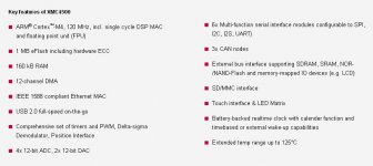
The Infineon XMC4500 will be easier to program than the NXP LPC4300 asymetric core (M4 + M0) and SGPIO.
The Infineon XMC4500 has 6x Multi-function serial interface modules configurable to SPI, I2C, I2S, UART. It might thus provide the required serial interfaces for a 3-way stereo crossover :
- 1 x I2S (left and right inputs)
- 3 x I2S (crossover outputs)
- 1 x SPI (SPDIF receiver mode, ADC mode, ASRC mode, DACs mode, volume control, display)
- 1 x I2C if some chips require one
USB for communicating with a PC, for setting up the crossover. Possibly, the same USB as asynchronous audio input ?
Memory-mapped LCD display using the bus interface.
Looks promising !
P.S. 1
If the entire Microchip PIC32 product portfolio doesn't get very quickly an upgrade, similar to the 6x Multi-function serial interface modules configurable to SPI, I2C, I2S, UART, .... it will be the end of the Microchip PIC32. Currently it is unclear for me if only the recently introduced Microchip PIC32MX1 and PIC32MX2 have the I2S capability within SPI, or if such I2S capability within SPI is now present on the whole Microchip PIC32 product portfolio.
P.S. 2
With all those new Cortex-M4 coming with flexible and configurable serial interfaces, supporting I2S, the recently introduced STM32 F4 looks quite rigid with only two I2S. And quite paradoxal, as it has a nice audio clocking scheme. Will we see a STM32 F4 upgrade, shortly ?
P.S. 3
What about T.I. LM4F1xx and LM4F2xx Cortex-M4 ? How many I2S ?
Attachments
Last edited:
For ICE, I think you could try using the USB-JTAG (or USB-SWD) half of this board:
New LPC1343 LPCXpresso board OM11048 NXP ARM Cortex FREE SHIPPING | eBay
Its cheaper than getting a stand-alone ICE and you get the 72MHz M3 thrown in for free
New LPC1343 LPCXpresso board OM11048 NXP ARM Cortex FREE SHIPPING | eBay
Its cheaper than getting a stand-alone ICE and you get the 72MHz M3 thrown in for free
Next up - Atmel
Atmel has announced sampling of its Cortex M4s - production due 2Q 2012. 120MHz, datasheet here : http://www.atmel.com/Images/11100.pdf
<edit> From a quick scan of the DS, not really interesting at all for audio - just one I2S, only full speed USB.
Atmel has announced sampling of its Cortex M4s - production due 2Q 2012. 120MHz, datasheet here : http://www.atmel.com/Images/11100.pdf
<edit> From a quick scan of the DS, not really interesting at all for audio - just one I2S, only full speed USB.
Last edited:
I took a skim through the SAM4S datasheet a week or two ago and didn't see a good way of repurposing another peripheral---such as the PIO---to provide I2S either.
Zero on the block diagrams. The datasheets do have a presence bit for a single I2S module so perhaps TI plans to add a dedicated peripheral. The four SSI units are close to what one needs in that you get BCLK and data. But on a quick look I'm not seeing a good story for LRCK as there doesn't seem to be a way to rig SSIFss to have the necessary semantics.What about T.I. LM4F1xx and LM4F2xx Cortex-M4 ? How many I2S ?
Last edited:
Microchip updated their SPI block, adding the "audio mode" configuration bit for converting the Slave-Select pin into a LRCK pin.
They did it for the newly introduced PIC32MX1xx family and PIC32MX2xx family, equipped with 2 SPI.
The PIC32MX220F032B has thus 28 pin, and is equipped with two SPI that can be turned into two I2S. It is available in PDIP package with the "I/SP" suffix, ideal for hobbyists and one-shot projects.
Don't know yet if the same evolution will occur for largers PIC32 chips like the PIC32MX5xx and PIC32MX6xx featuring up to 4 SPI.
With the PIC32MX220F032B, you can implement a crossover "trench" using the following resources allocation :
- SPI_1 used as I2S, taking the full spectrum signal as input and delivering a filtered signal as output
- SPI_2 used as SPI for accessing the DACs internal registers.
The annoyance of such "trench" architecture is that you need two PIC32 chips for making a 2-way crossover, and three PIC32 chips for making a 3-way crossover. How to easily reprogram two or three PIC32 chips on a board ? How to organize the inter-chip communication if reprograming must be done using USB ?
With a little more effort, with the PIC32MX220F032B, you can implement a complete 2-way crossover using the following resources allocation :
- SPI_1 used as I2S, taking the full spectrum signal as input and delivering the lowpass filtered signal as output
- SPI_2 used as I2S, taking no input signal and delivering the highpass filtered signal as output
- a bit-banging SPI implementation using GPIOs for accessing the DACs internal registers (I guess Microchip website has sample code for this).
The 2-way crossover looks tempting. Only one PIC32 chip needed. Easy to program, easy to maintain.
The Microstick II (DM330013-2) is a small development kit made by Microchip, hosting a PIC32MX220F032B chip. The Microstick II (DM330013-2) actually supports all PIC32 SPDIP packaged devices. You should get it for 29.04 eur from Mouser.
DM330013-2 Microchip Technology Development Boards & Kits - PIC / DSPIC
If you destroy the PIC32 SPDIP chip, you can buy a new one from Mouser for 2.92 eur, and plug it into the 28-pin socket.
PIC32MX220F032B-I/SP Microchip Technology Microcontrollers (MCU)
Need to verify if the resulting PIC32 I2S can remain in sync and work as slaves, using a Wolfson WM8580 CODEC as master. The WM8580 has SPDIF-in, stereo Analog-in, and six Analog-out.
Need to verify if the PIC32 I2S can work with a 16-bit audio word lenght at the input, and a 24-bit audio word lenght as output.
Need to verify if the PIC32 I2S get some buffering, for off-loading the CPU when dealing with 32-bit or 48-bit frame lenghts.
Everything considered, I think the new PIC32MX2xx family is a great new toy to experiment with.
For testing the I2S protocol, I'll attach the MikroE Audio Codec Board - Proto. Audio Codec Board - PROTO - WM8731 Development Tool - mikroElektronika
I think I'll start with the PIC32, then switch to the ARM Cortex-M4 when the Infineon XMC family becomes available.
Or maybe stay with the PIC32 if Microchip manages to provide an "audio mode" for their SPI in their larger PIC32 chips, currently up to 4 SPI in a chip.
Last edited:
The four SSI units are close to what one needs in that you get BCLK and data. But on a quick look I'm not seeing a good story for LRCK as there doesn't seem to be a way to rig SSIFss to have the necessary semantics.
On the LPC parts I've successfully used a timer to generate the WS. Only tried that in master mode though and getting the correct phase is a little tricky
I had to put in some software delay empirically. Haven't quite figured a way yet to do it without human feedback in the setting of the delay.Good question.does the PIC32 have a fast multiply or MAC capability ?
From the data sheet: Single-cycle (MAC) 32x16 and two-cycle 32x32 multiply
It does make me wonder how they distinguish the dsPIC from the PIC32 families.
Tricky to handle an I2S input that way, though.I've successfully used a timer to generate the WS
Even with the LPC4300's rather generous hardware resources I'm coming up against the part's limits. Both the I2S and SGPIO peripherals are convenient in that the input BCLK can be passed through as the output BCLK, meaning one doesn't have to implement an ASRC. However, it does not appear possible to pass an input clock directly from one peripheral to the other. In theory one can get around this by routing an SGPIO slice operating as an output clock to the GP_CLK pin and then sending that through the CGU to the I2S peripheral. But the approach is not especially attractive as it seems there are more valuable uses for GP_CLK. There's also the small difficulty that all current packages assign GP_CLK and I2S peripheral clocks to the same pin.A better way seems to be to do all I2S signalling with SGPIO. Nominally, that provides five three pin I2S lines, up to four of which can be inputs. That accomodates two I2S sources and a three way crossover. If you have three or more sources and a three way cross you either have to fan out BLCK and LRCK (not the end of the world, though it means more cost, complexity, and possibly additive jitter depending on how fanout is implemented and how the DACs are clocked), use a multichannel DAC so that BCLK and LRCK are shared across data lines (not the end of the world either, though it significantly restricts part choices compared to working with stereo DACs), or do external muxing of the inputs (not a big deal). It would be nice to have three I2S inputs and three outputs, but I've sufficiently little need for the third input I'd prefer to go with two inputs and three outputs and get a single chip solution for all I2S management.
The snag is I2S is really a four wire interface once you account for MCLK, meaning simple use of SGPIO is limited to four I2S lines with the output MCLKs having some amount of additive jitter from being buffered within the LPC. This isn't bad---I don't know of any other part which could handle MCLK generation this way---but four I2S is one less than I need to avoid multiple PCBs for scenarios that are only slightly different. One solution's to use an ESS DAC in asynchronous mode, obviating the need to pass MCLK around. Another is to use a dual input clock generator with a sufficient number of outputs. That requires some glue code to change the clock gen's input when changing between the I2S inputs and incurs the cost and complexity of the clock gen, though it does admit use of a jitter cleaner and gets the MCLK pins off the LPC. A nicer approach would be to use PLL0AUDIO on LPC. Unfortunately, the behavior of its bandwidth selection currently seems to be undocumented, though as it's a DPLL, one can probably get pretty low cutoffs and hence be able to pass a reasonably low jitter MCLK to SGPIO. No spec on how much jitter the internal routing and SGPIO output buffers would add but, given NXP bothered to implement a fractional PLL and CLKOUT, it seems safe to assume some design attention was paid here and that the jitter would probably be in 60ps period jitter, 200ps peak to peak range typical of low cost parts.
The limitation with this approach is the logical choice for an external MCLK input---such as that generated by a Wolfson WM8804 or WM8805 SPDIF receiver---is GP_CLK. This is fine, but there's only one GP_CLK pin. So switching between different external MCLKs means repurposing ENET_RX_CLK as an audio clock. ENET_RX_CLK is only available on the 180+ pin packages. ENET_TX_CLK could also be used, but it's assigned to the CLKOUT pin and one may want to use CLKOUT to deliver an MCLK. Since CLKOUT would probably also be the SGPIO clock in this case one can use that 16th SGPIO slice that isn't being used for a BCLK, LRCK, or SDATA to deliver a second MCLK. There's no spec on how much skew you'd get from this but a safer option would be to fan out the output LRCK (since it's the lowest bandwidth signal among the I2S outputs) and use the two slices that frees up to deliver MCLKs to DACs. It then seems most natural to use CLKOUT as a clock supply for the second I2S input.
If you add all that up I think this means it's probably just viable to implement a three way crossover with a SPDIF input and an auxillary I2S input which could be used for an ADC or such in a single LPC4300. If one needs a third input it's probably still workable in a single chip, but only if all you need is a two way crossover. Similarly, if it's a four way crossover then external muxing is required for multiple inputs. The only thing I can't fit in to SGPIO is a second LRCK pin---that's needed for the variable Fs we were discussing a few posts back since it requires LRCKs at different rates. Have to take a look and confirm there's a way to get a clock synchronous to SGPIO BCLK over to an SSP, SPIFI, USART, or similar peripheral but---worst case---it should be possible to bit bang an extra LRCK.
- Status
- This old topic is closed. If you want to reopen this topic, contact a moderator using the "Report Post" button.
- Home
- Source & Line
- Digital Line Level
- Open Source DSP XOs