One way to approach the software side is to define an XML schema (XSD) describing the supported XO building blocks (channels, filters), their configuration options, and the ways they can, and hence cannot, be combined. XML documents that match it can serve as the files describing your XO design, which can be saved, shared with others etc.
The essential part then is to find a way to translate these XMLs to instruction sets that can be executed by the DSP board, and preferably vice versa as well. Not sure if the latter is very feasible though.
One advantage is that it would turn the ultimate goal of the GUI's XO design section into one of manipulating the contents of an XML file. Especially for a POC this part could temporarily be replaced by any tool that is capable of doing this.
Also, it could simplify the task of converting XO/filter designs made in other tools, as one wouldn't have to worry about the target DSP's internals. Valid XML would be all the converter has to produce.
Anyway, just my two cents...")
The essential part then is to find a way to translate these XMLs to instruction sets that can be executed by the DSP board, and preferably vice versa as well. Not sure if the latter is very feasible though.
One advantage is that it would turn the ultimate goal of the GUI's XO design section into one of manipulating the contents of an XML file. Especially for a POC this part could temporarily be replaced by any tool that is capable of doing this.
Also, it could simplify the task of converting XO/filter designs made in other tools, as one wouldn't have to worry about the target DSP's internals. Valid XML would be all the converter has to produce.
Anyway, just my two cents...
For anyone who's been shying away from Cortex M0 as DSP because the packages aren't quite DIY-friendly enough, this will come as welcome relief :
NXP Cortex-M0 Microcontrollers in High-Volume TSSOP and SO Packages Target 8/16-bit Applications :: NXP Semiconductors
NXP I reckon is the DIYers friend - who on earth apart from a DIYer would be designing with a DIL28 0.6" pitch package MCU? (Datasheets weren't available last time I checked.)
NXP Cortex-M0 Microcontrollers in High-Volume TSSOP and SO Packages Target 8/16-bit Applications :: NXP Semiconductors
NXP I reckon is the DIYers friend - who on earth apart from a DIYer would be designing with a DIL28 0.6" pitch package MCU?
(Datasheets weren't available last time I checked.)More details from ARM on the DIL Cortex M0s :
Hey Hobbyists, dust off your breadboards - DIP package is back; - ARM Community
Hey Hobbyists, dust off your breadboards - DIP package is back; - ARM Community
NXP now has the updated datasheet which includes the 20- and 28-pin M0 parts. Oddly though if you go looking for it on the M0 microcontrollers section, you hit a 404 error
http://www.nxp.com/documents/data_sheet/LPC1110_11_12_13_14.pdf
http://www.nxp.com/documents/data_sheet/LPC1110_11_12_13_14.pdf
Here's an illuminating chat with an EDA guru about the way computing is being constrained to move in the direction of lower power - of course, using ARM.
Gary Smith EDA talks about the state of the ARM industry – ARMdevices.net
Gary Smith EDA talks about the state of the ARM industry – ARMdevices.net
I saw the video showing Gary Smith in post #45 above. Liked the idea of "instant on, normally off" computing. Liked the idea of the current drain becoming the most important specification. Got amazed when he described a 400 MHz clock as ideal nowadays, and Gigahertz clocks to be considered as a joke. I liked the idea of the PC reducing to a niche, in front of mobile phones, tablets and new generation computing devices becoming mainstream. However, I could not catch the objection about the Cloud at 9:22 in the video. Can someboby explain it to me ?
Where do we go, actually ?
A quad core Cortex-A7 accompanied by a PowerVR SGX, both clocked at 400 MHz nominal, that you can push to 800 MHz ?
Worth looking at BeagleBone, basing on a TI AM3358 ARM, currently single core Cortex-A8. http://www.ti.com/product/am3358
Two Multichannel Audio Serial Ports Supporting Time Division Multiplexing (TDM), Inter-IC Sound (I2S), and similar Formats.
Expected retail price of $89.
Will execute 2048-tap FIRs in stereo at 96 kHz with 32x32+64=64 math ?
Last edited:
I've heard this idea about mobile computing taking over but the fact is for serious computationally intensive applications, as things get more efficient, there will still be high demand for whatever can be done with a couple hundred watts. Some people don't realize that the world is not advancing simply by browsing the internet and streaming some video.
$5 Cortex-A8 SoC aims to take on ARM9 in the embedded market - News - Windows for Devices
It says there will be T.I. AM335x chips (presumably not equipped with the PowerVR SGX) costing as little as $5 in volume.
Add some Flash, run from internal RAM, and you get more computing power than a DSP56725, and more precison thanks to the 32x32+64=64 math.
On the other hand, the DSP56725 has a better audio DSP connectivity, featuring four I2S lanes.
What is the STM32 F4 price, in volume ?
The STM32 F4 is a 90 nanometer Cortex-M4 clocked at 168 MHz featuring :
- Up to 1 Mbyte of Flash memory
- Up to 192+4 Kbytes of SRAM including 64-Kbyte of CCM (core coupled memory) data RAM
- Flexible static memory controller supporting Compact Flash, SRAM, PSRAM, NOR and NAND memories
- Up to 3 × I2C interfaces (SMBus/PMBus)
- Up to 4 USARTs/2 UARTs (10.5 Mbit/s, ISO 7816 interface, LIN, IrDA, modem control)
- Up to 3 SPIs (37.5 Mbits/s), 2 with muxed full-duplex I2S to achieve audio class accuracy via internal audio PLL or external clock
- 2 × CAN interfaces (2.0B Active)
- 1 x SDIO interface
The two full-duplex I2S enable building an inexpensive "parallel" xover like analog xovers are (thanks abraxalito for the idea).
Put one F4 as stereo equalizer and/or room equalizer.
Put one F4 as stereo sub & bass stereo channels processor.
Put one F4 as stereo medium & tweeter channels processor.
Is there a single-cycle 32x32+64=64 multiplier-accumulator ?
If yes, three F4 chips would deliver 504 DSPMips combined.
There could be a 512-tap FIR in the room equalizer.
There could be a 256-tap FIR in each channel, for individually equalizing the speaker drivers gain and phases.
Okay, I confess a DSP56725 delivering 500 DSPMips, only costing $6.05, also can do this.
Here, with the F4, you would execute 32x32+64=64 math instead of 24x24+48=48 math.
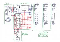
Attached is a design proposal. Anyone interested ?
The STM32 F4 is a 90 nanometer Cortex-M4 clocked at 168 MHz featuring :
- Up to 1 Mbyte of Flash memory
- Up to 192+4 Kbytes of SRAM including 64-Kbyte of CCM (core coupled memory) data RAM
- Flexible static memory controller supporting Compact Flash, SRAM, PSRAM, NOR and NAND memories
- Up to 3 × I2C interfaces (SMBus/PMBus)
- Up to 4 USARTs/2 UARTs (10.5 Mbit/s, ISO 7816 interface, LIN, IrDA, modem control)
- Up to 3 SPIs (37.5 Mbits/s), 2 with muxed full-duplex I2S to achieve audio class accuracy via internal audio PLL or external clock
- 2 × CAN interfaces (2.0B Active)
- 1 x SDIO interface
The two full-duplex I2S enable building an inexpensive "parallel" xover like analog xovers are (thanks abraxalito for the idea).
Put one F4 as stereo equalizer and/or room equalizer.
Put one F4 as stereo sub & bass stereo channels processor.
Put one F4 as stereo medium & tweeter channels processor.
Is there a single-cycle 32x32+64=64 multiplier-accumulator ?
If yes, three F4 chips would deliver 504 DSPMips combined.
There could be a 512-tap FIR in the room equalizer.
There could be a 256-tap FIR in each channel, for individually equalizing the speaker drivers gain and phases.
Okay, I confess a DSP56725 delivering 500 DSPMips, only costing $6.05, also can do this.
Here, with the F4, you would execute 32x32+64=64 math instead of 24x24+48=48 math.
Attached is a design proposal. Anyone interested ?
Attachments
I could not catch the objection about the Cloud at 9:22 in the video. Can someboby explain it to me ?
That's also the only part of the video that left me confused. He was talking about homogenous and heterogenous computing and he implied that the cloud model was the former rather than the latter. I couldn't make the jump that he was seeing - to me the cloud is heterogenous - its isomorphic to ARM's big.LITTLE with the LITTLE in your hand and the big in the cloud.
Yeah its very interesting (particularly the low price) but the ARM CPU is rather a different one (ARM11, 700MHz), the older generation designed more for applications than pure embedded.
Here's a really fascinating video on the LPC43XX's smart peripheral functions - the sheer number of I2S outputs will appeal to lots of audio guys and gals who want to do multichannel. Rob Casaro seems to me to be one disruptive thinker
Configurable and Virtual Peripherals SGPIO and SCT - YouTube
Here's a really fascinating video on the LPC43XX's smart peripheral functions - the sheer number of I2S outputs will appeal to lots of audio guys and gals who want to do multichannel. Rob Casaro seems to me to be one disruptive thinker
Configurable and Virtual Peripherals SGPIO and SCT - YouTube
Thanks for that. The SGPIO looks very useful, and I think he said there are 8 on the chip, so that's potentially 16 stereo DAC chips or even more channels if you're willing to use multichannel chips (assuming the clock rates of the SGPIO can keep up).Here's a really fascinating video on the LPC43XX's smart peripheral functions - the sheer number of I2S outputs will appeal to lots of audio guys and gals who want to do multichannel.
Yeah its very interesting (particularly the low price) but the ARM CPU is rather a different one (ARM11, 700MHz), the older generation designed more for applications than pure embedded.
Here's a really fascinating video on the LPC43XX's smart peripheral functions - the sheer number of I2S outputs will appeal to lots of audio guys and gals who want to do multichannel. Rob Casaro seems to me to be one disruptive thinker
Configurable and Virtual Peripherals SGPIO and SCT - YouTube
Hoes does it handle a 24/32 bit I2S stereo signal. It would need a 64 bit register to do that or can you cascade two of its 32 bit serial registers ??
regards
Trevor
Excellent point, Trevor. Now that you point it out, it just might be true that only I2S mono signals can be supported. However, I get the impression that most of the people here are only interested in mono anyway, or at least have no interest in multichannel. So, perhaps 8 mono I2S outputs would be ideal for the majority of folks here.Hoes does it handle a 24/32 bit I2S stereo signal. It would need a 64 bit register to do that or can you cascade two of its 32 bit serial registers ??
I think the real test is for someone to get an evaluation board with this particular ARM and write some firmware to use the SGPIO ports in an audio application. Only then will we know for sure what can be accomplished.
From the LPC4350 datasheet:
Features
• Each SGPIO input/output slice can be used to perform a serial to parallel or parallel to serial data conversion.
• 16 SGPIO input/output slices each with a 32-bit FIFO that can shift the input value from a pin or an output value to a pin with every cycle of a shift clock.
• Each slice is double-buffered.
• Interrupt is generated on a full FIFO, shift clock, or pattern match.
• Slices can be concatenated to increase buffer size.
• Each slice has a 32-bit pattern match filter.
I'd say this says you can capture 32bits per channel because its got a 32bit wide FIFO. It could also for example be used to create 'multi-I2S' where there's more than one bit indicating channel.
On the video ARM Cortex-M4 demo from DSP Concepts - YouTube, at 0:48 you can see the LPC43xx board having an audio CODEC surrounded by four stereo 3.5 mm jacks.It just might be true that only I2S mono signals can be supported. However, I get the impression that most of the people here are only interested in mono anyway, or at least have no interest in multichannel. So, perhaps 8 mono I2S outputs would be ideal for the majority of folks here. I think the real test is for someone to get an evaluation board with this particular ARM and write some firmware to use the SGPIO ports in an audio application. Only then will we know for sure what can be accomplished.
On a chinese NXP webpage it says "The LPC4300’s SGPIO, available for the first time, allows a developer the flexibility to interface to any non-standard serial interface or to mimic multiple standard serial interfaces (such as I²S, TDM for multi-channel audio, I²C and more)."
When designing silicon, you must set a limit to the registers lenghts. It sounds thus healthy and logic to have the SGPIO architectured around 32-bit registers, not 64-bit registers, not 128-bit registers, and not 256-bit registers. With the LPC43xx GPIO, when you need to generate frames containing more than 32 bits (like I2S 2x24 bits, or TDM), you use the M0 as sub-frame sequencer. Robert Casaro from NXP is clear about this is his youTube video http://www.youtube.com/watch?v=2KPZ3TCcKVY.
Take TDM as example. The frame contains 8 x 32-bit words. The SGPIO needs to initiate a DMA transaction (or an interrupt) at 8 times the audio sampling frequency. Say you are using TDM at 48 kHz, the SGPIO will initiate a DMA transaction (or an interrupt) at 384 kHz. Say you are using TDM at 96 kHz, the SGPIO will initiate a DMA transaction (or an interrupt) at 768 kHz.
Using parallel I2S lanes instead of TDM only requires the SGPIO to initiate a DMA transaction (or an interrupt) at 2 times the audio sampling frequency. Which means 96 kHz at a 48 kHz sampling frequency, or 192 kHz at a 96 kHz sampling frequency.
Currently, the only LPC43xx chips that are available, require the deployment of a system bus and the associated buffers for accessing external Flash (and external RAM). You can see them on the youTube video. Currently the BOM cost for a xover built around the NXP43xx is extravagant (high) compared to the BOM cost of a xover built around a 50 MIPS ADAU1701 (miniDSP), or a 500 MIPS DSP56725. NXP doesn't want the NXP43xx to carry this kind of negative image. This is the reason they won't make this board more available than it is currently. No doubt there is another board in the pipeline, significantly smaller, basing on a LPC43xx chip having internal Flash, to be sold in volume for competing with the STM32 F4 Discovery board.
Currently, quite interesting in the ARM world, is the STM32 F4 chip, a Cortex-M4 having built-in Flash and RAM, clocked at 168 MHz, providing three SPI, two of them having the capability to operate as I2S. With two I2S lanes, you can do a stereo 2-way xover. For a stereo 3-way or 4-way xover, you can put two STM F4 chips in parallel. There is a STM32 F4 Discovery board available from Mouser, priced at 13.96 eur. A possible xover architecture would be a STM32 F4 as pre-processor (executing a FIR-based room equalizer and a IIR-based Linkwitz Transform) followed by two STM32 F4 in parallel as crossovers (each STM32 F4 dealing with stereo 2-ways, all channels benefitting from a FIR-based driver linearization). The cost for one STM32F407VET6 is 6.84 eur in small qualtities from Mouser. The total BOM cost a stereo 4-way xover featuring three such chips stays reasonable. The advantage of the ARM Cortex-M4 is that your FIRs and IIRs are done in fixed point 32x32+64=64 math, single cycle.
There are inexpensive Cortex-M3 chips produced by NXP, featuring two buffered SSPs. They could be used for emulating I2S. This way you get two pseudo-I2S per chip. If you need SPI as extra (like for controlling the DACs volumes), you'l need to bit-bang it. Mouser sells the NXP LPC1313FBD48/01 for 2.65 eur in small quantities. The disadvantage of such M3 solution is a) a somewhat fragile I2S as you need to manually sync the LRCK, b) a 72 MHz clock frequency (compared to 168 MHz with STM32 F4), c) the fixed point 32x32+64=64 math is not single cycle (actually, there is no register acting as accumulator) and d) the need to bit-bang the SPI for the DACs volumes.
Now, this being said, I had a look on beagleBone featuring the AM335x chip manufactured by T.I. There are up to two Multichannel Audio Serial Ports (McASP) supporting TDM, I2S and SPDIF natively. A single AM335x chip can thus talk to a 8-channel DAC. If you don't like TDM, that's not an issue as there are up to four Serial Data Pins per McASP. You thus can use four parallel I2S lanes. You may use the second Multichannel Audio Serial Port as direct SPDIF-in in case you don't insert an ASRC. T.I. is launching the AM335x family, saying there will be members costing as little as 5.00 dollars in volume. Compare the price with the STM32 F4 chips. Amazing. For an audio xover, the 64 KB on-chip RAM may suffice. CPU clock is an amazing 500 MHz, so no question of running from Flash. The external Flash memory can be a tiny serial Flash chip, from where the AM335x can boot. How to do this, actually ? But wait a minute, this way, everybody will be able to read the external Flash, copy it, and rob the software. What to do ? Does it mean NOGO ? Not at all if the idea is to make the xover software open-source. This makes me say that currently, the AM335x is the best single-chip solution for an open-source DSP XO. Actually, the AM335x is a DSP56725 killer.
With a AM335x, a serial Flash and a 8-channel DAC, within 6 months, you'll get a credit-card sized open-source DSP XO priced 49 dollar. Look how inefficient, fragile and more costly is to emulate four I2S lanes using two or three NXP LPC1313FBD48/01 chips. Look how more costly it is, getting four I2S lanes using two or three STM32F407VET6 chips. Look how difficult it is to maintain an application that's spread on two or three chips. How would you program and debug those chips ? The Segger J-Link supporting SWD is not the cheapest tool.
Clearly, in the absence of LPC43xx chips, the AM335x is the winner.
Now, this being said, as soon as there is a LPC43xx chip available, it is worth having a look to it. I'm slowly getting to the idea that a LPC43xx chip will come, essentially the same price as the AM335x chip, featuring a built-in Flash memory as main sales argument, especially if there is a software piracy protection feature. With the LPC43xx, you would trade MIPS against compacity (built-in Flash) and software protection. Not a bad deal, actually. But wait a minute, as there are two CPU cores in a LPC43xx chip, aren't we obliged to use the Segger J-Link as SWD as programming and debug tool ? This is another factor preventing the LPC43xx chips to widely access the embedded market quickly. They are dualcore. They need a SWD programming and debug tool. Embedded Artists being in charge of designing an inexpensive LPC43xx board, they need to revise their Embedded JTAG (LPC-LINK) and migrate it to SWD. We thus love the LPC43xx chip, currently we don't need it to be significantly cheaper than the T.I. AM335x chip, and currently we are waiting for a LPC43xx LPCXpresso Board from Embedded Artists featuring a LPC43xx with on-chip Flash, and featuring the required multicore software development environment thanks to a so-called Embedded SWD (SWD-LINK).
It is like in the automobile sector. You can't market a new car featuring a new engine and a new body. The LPC43xx is introducing two major changes at the same time : Flash-less and dualcore. Possible three revolutions if you were a FDSP56K programmer, with the migration from DSP56K to ARM. That's too many changes. NXP needs to launch a LPC43xx chip with on-chip Flash, and Embedded Artists need to launch a software SDK streamlining dualcore software development, associated to a cheap LPCXpresso Board.
Every week passing, will cause people opting for the T.I. AM335x chip instead of the NXP LPC43xx chip. Must say that with a 500 MHz clock frequency, the T.I. AM335x chip establishes as "the" Freescale DSP56725 killer.
Last edited:
As far as I can recall from the NXP videos, yes its single-cycle multiply, single precision (32bit). The max clock frequency depends on the vendor - STM is 168MHz, NXP 180MHz. The wild card is TI, although they only specify 80MHz I reckon their part might well run much faster than advertised as they've built it in 65nm.
I have done quite a lot of DSP programming in fixed point, and I would not refer to it as an advantage. In terms of power usage and cost of silicon, fixed point does have advantages, but in terms of audio filter processing I'd say that floating point would have the advantage in all but the simplest crossovers.The advantage of the ARM Cortex-M4 is that your FIRs and IIRs are done in fixed point 32x32+64=64 math, single cycle.
EDIT: Upon rereading this, I guess maybe you're saying that the advantage is the 64-bit aspect, not the fixed point aspect. I usually work with a DSP that has 40-bit and 80-bit accumulators, so at first I did not see your point. I guess that when you press a general purpose processor into DSP work, you typically have to deal with smaller 32-bit registers, but with special purpose DSP chips you have the advantage that the processor is already designed with enough bits of overhead to handle calculations properly. This suggests to me that a great option would be one of the Texas Instruments chips that combines both an ARM and TMS320 DSP in the same package. Perhaps overkill for a crossover, but certainly the DSP will have appropriate instructions and registers for filters.
I2S has at least three signals, if not five, so how do you get four parallel I2S lanes from two McASP ports? Also, when you speak of these Serial Data Pins, are you suggesting that the processor bit-bang these pins to implement I2S?I had a look on beagleBone featuring the AM335x chip manufactured by T.I. There are up to two Multichannel Audio Serial Ports (McASP) supporting TDM, I2S and SPDIF natively. A single AM335x chip can thus talk to a 8-channel DAC. If you don't like TDM, that's not an issue as there are up to four Serial Data Pins per McASP. You thus can use four parallel I2S lanes.
I have worked with the TI McBSP ports and have studied the McASP ports. I would suggest that the most you could hope for with up to two McASP ports is to implement up to two I2S lanes.
If you'd care to explain how a single McASP port can implement two parallel I2S lanes, or even if you can just point to a specific page in the Texas Instruments documentation which gives any clue as to how this could be pulled off, then I would be seriously interested in learning a new technique.
Last edited:
- Status
- This old topic is closed. If you want to reopen this topic, contact a moderator using the "Report Post" button.
- Home
- Source & Line
- Digital Line Level
- Open Source DSP XOs