I was up at 5:00 this morning. And earlier weekdays.
Enjoy your stay,
Patrick
Oh boy Patrick, your an expert with electronics but I sure could help you out with that nasty early rising.
The hour of rising is directly proportional to the square of alcohol volume consumed the night before

Will eventually get the Sens in full differential audio next week btw
Oh boy Patrick, your an expert with electronics but I sure could help you out with that nasty early rising.
The hour of rising is directly proportional to the square of alcohol volume consumed the night before
Will eventually get the Sens in full differential audio next week btw
Well although I may not stay up thereafter, I find my own body works differently, more of a reciprocal to the square of ethanol consumed, after a constant is added of order three hours.
It can be useful though to be able to respond to e mail in the earliest morning, giving clients the illusion that one is up continuously.
what you guys think about the 2sk715 from sanyo to substitute the 2sk170 ?
It has higher forward transfer admittance (50mS), and lower gate drain capacitance (3pf). And is also low noise.
http://www.onsemi.com/pub_link/Collateral/EN2543-D.PDF
It has higher forward transfer admittance (50mS), and lower gate drain capacitance (3pf). And is also low noise.
http://www.onsemi.com/pub_link/Collateral/EN2543-D.PDF
That looks like a nice part, similar to the BF862 but in through-hole. Low voltage however, so that requires some care.what you guys think about the 2sk715 from sanyo to substitute the 2sk170 ?
It has higher forward transfer admittance (50mS), and lower gate drain capacitance (3pf). And is also low noise.
http://www.onsemi.com/pub_link/Collateral/EN2543-D.PDF
2sk932 is the smd version of 2sk715 and is cheaper.
BF862 has very good characteristics, and higher Vds (20v).
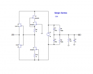
Patrick I am doing some tests with your circuit ( CEN ) , I think it can be very good solution for PCM1794 as this type of DAC has very high output impedance.
The major source of distortion of the CEN with this type of DACs is the gate to drain non linear capacitance of the Jfets, I am trying to come up with a simple solution that do not add much complexity and maintain the excellent stability of your circuit.
BF862 has very good characteristics, and higher Vds (20v).
Patrick I am doing some tests with your circuit ( CEN ) , I think it can be very good solution for PCM1794 as this type of DAC has very high output impedance.
The major source of distortion of the CEN with this type of DACs is the gate to drain non linear capacitance of the Jfets, I am trying to come up with a simple solution that do not add much complexity and maintain the excellent stability of your circuit.
The distortion mechanism has been discussed in some detail in my article which you can download (free) from Jan Didden's Linear Audio website.
The easiest way to reduce non linear capacitance is to use SEN with BF862, cascoded with J111.
In Spice simulation, the distortion is as low as -120dB or thereabouts.
But the distortion even in the original SEN is very very low, that you may not hear any difference. More an intellectual challenge.
And cascoding thus make it more prone to oscillation.
Try it out in Spice for yourself.
Patrick
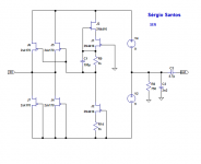
This is what I have for now. The stage based on 2n4416 act as a buffer between the gate non linear currents of the input Jfet (2sk170 , 2sj74) and the ground.
With a infinite output impedance source the distortion is near zero, with the same conditions the normal CEN have 0.005% because of the Crss non linearities.
The distortion with a input impedance of 200K , 8ma p-p and 6 Volts P-P output is 0.00002%.
I am looking for a substitute for the 2n4416.
With a infinite output impedance source the distortion is near zero, with the same conditions the normal CEN have 0.005% because of the Crss non linearities.
The distortion with a input impedance of 200K , 8ma p-p and 6 Volts P-P output is 0.00002%.
I am looking for a substitute for the 2n4416.
Attachments
I have try to cascode the input Jfet , but as you said, doing that causes stability issues.
And stability is the main reason to use this type of circuit.
I prefer the solution that I present in post #1370. I have include the LTspice file. Try it.
edit: for ascurate distortion test and ftt, go to control panel in LTspice and disable compression.
Patrick I am reading your article.
And stability is the main reason to use this type of circuit.
I prefer the solution that I present in post #1370. I have include the LTspice file. Try it.
edit: for ascurate distortion test and ftt, go to control panel in LTspice and disable compression.
Patrick I am reading your article.
Last edited:
Patrick I am doing some tests with your circuit ( CEN ) , I think it can be very good solution for PCM1794 as this type of DAC has very high output impedance.
Hi, Sergio,
As you know, one of the complications in designing an I/V for the PCM1794A is how to handle the 6.2mA output bias current. The need to handle this current keeps rearing it's ugly head in the many grounded base/gate circuits that I've designed, where it causes severe D.C. current imbalance and D.C. voltage offset. Summing an offsetting current at the I/V stage's input via an external C.C.S. is one solution, but this adds additional complexity and represents one more element which must be hand trimmed.
Another issue, I feel, complicating the use of grounded base/gate type I/V circuits is the band-limiting of the input signal current. I'm not so concerned about about I/V stage upper harmonics, which are often relatively low and/or out-of-band in grounded base/gate. I'm more concerned about in-band IMD products. Perhaps, the best way to reduce IMD is to band-limit the input signal before applying it to the stage in question. However, simply placing a small capacitor from the DAC's current output to ground seems to upset the grounded base/gate type circuit's THD performance. I suspect this may be because such a bypass cap. transforms what was a high DAC source impedance (good) in to a much lower source impedance (bad). These issues keep driving me back to a simple, low value, passive resistor I/V followed by voltage amplifiction, at least for DAC chips such as the PCM179x series, and the AD1955.
Grounded base/gate circuits attract me becuse of their elegance and wideband performance, but then seem to get tripped up by the implementation details. I suspect that majority of my attraction has to do with their ability to track the wideband DAC output signals relatively accurately, hence, this circuit's popularity in RF signal applications. However, do we really desire accuracy in the handling of signal content above 20KHz, or do we really simply want to ensure that above band signal content does not cause harm to the in band 20Hz-20KHz content? Just my thoughts.
Last edited:
Hi Ken,
There is no need to bother too much about the IMD, as the switching frequency of the DAC are much higher than the audio band, the IMD products will be very futher away from the audio band .
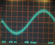
I posted a picture of a 5khz sine modulated by 500khz pulse, as you can see, there is harmonics produced by the IMD around the 500khz , 1Mhz and so one but nothing in the audio band.
I think that the high frequency noise from the output of the DAC can be problematic with I/V converters that use feedback , but not with this type of I/V converters, thats the reason I am so interested in this type of I/V converters, of course passive resistor I/V is also a good option , at least with pcm1794 as we see in another thread, but do not forget to filter the high frequency noise before the feedback amplifier.
And as you said adding a capacitor to ground in the input will bring down the impedance , and that is a bad thing, we are better without it.
I will talk about the bias current later.
the 2º and 3º image is the output of the PCM1794 I/V without output capacitor and with 2n2 in parallel with 750 ohms.
There is no need to bother too much about the IMD, as the switching frequency of the DAC are much higher than the audio band, the IMD products will be very futher away from the audio band .
I posted a picture of a 5khz sine modulated by 500khz pulse, as you can see, there is harmonics produced by the IMD around the 500khz , 1Mhz and so one but nothing in the audio band.
I think that the high frequency noise from the output of the DAC can be problematic with I/V converters that use feedback , but not with this type of I/V converters, thats the reason I am so interested in this type of I/V converters, of course passive resistor I/V is also a good option , at least with pcm1794 as we see in another thread, but do not forget to filter the high frequency noise before the feedback amplifier.
And as you said adding a capacitor to ground in the input will bring down the impedance , and that is a bad thing, we are better without it.
I will talk about the bias current later.
the 2º and 3º image is the output of the PCM1794 I/V without output capacitor and with 2n2 in parallel with 750 ohms.
Attachments
Hi, Sergio,
Yes, the IMD products of 500KHz and 5KHz will be far up at 495KHz and 505KHz. My IMD worries are over the many closely spaced ultrasonic image frequencies produced at multiples of the sampling (or, oversampling) rate. Which, of course, could produce a range of audible baseband components. So, no worries about 5KHz and 500KHz, but worries about 500KHz and 501KHz. The IMD components themselves could even intermodulate with each other. That's the basis of my concern. So, while circuit linearity at high frequencies helps us here, as does bandlimiting the input signal. Grounded base/gate circuits are good at the former, but make difficult to implement the latter.
Yes, the IMD products of 500KHz and 5KHz will be far up at 495KHz and 505KHz. My IMD worries are over the many closely spaced ultrasonic image frequencies produced at multiples of the sampling (or, oversampling) rate. Which, of course, could produce a range of audible baseband components. So, no worries about 5KHz and 500KHz, but worries about 500KHz and 501KHz. The IMD components themselves could even intermodulate with each other. That's the basis of my concern. So, while circuit linearity at high frequencies helps us here, as does bandlimiting the input signal. Grounded base/gate circuits are good at the former, but make difficult to implement the latter.
This is the SEN version with the conditions of post#1370 the distortion is 0.00009% with 2sk170
This is what I was trying to do with #998. Your version is better in simulation. Does it work?
On the quest for an alternative to batteries...
How about a low frequency (say <100Hz) switched capacitor power supply using low output capacitance solid state relays?
i.e. use solid state relays to switch both sides of a bucket capacitor from a supply to a floating reservoir capacitor followed by a floating regulator.
This one has 1.1pF typical output capacitance:
http://www1.futureelectronics.com/doc/CALIFORNIA EASTERN LAB/PS7200R-1A-F3-A.pdf
So, 4 relays, 2 capacitors and a regulator per floating supply. Some shared logic to sequence the relays. Resulting in 2.2pF stray capacitance from each floating supply to ground.
Any chance of this working?
Hi, Sergio,
Yes, the IMD products of 500KHz and 5KHz will be far up at 495KHz and 505KHz. My IMD worries are over the many closely spaced ultrasonic image frequencies produced at multiples of the sampling (or, oversampling) rate. Which, of course, could produce a range of audible baseband components. So, no worries about 5KHz and 500KHz, but worries about 500KHz and 501KHz. The IMD components themselves could even intermodulate with each other. That's the basis of my concern. So, while circuit linearity at high frequencies helps us here, as does bandlimiting the input signal. Grounded base/gate circuits are good at the former, but make difficult to implement the latter.
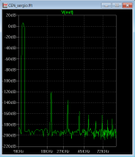
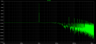
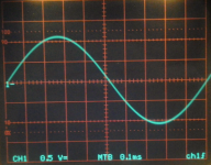
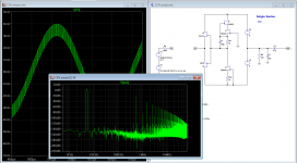
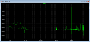
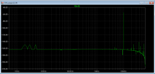
Ken , I have made a test with the circuit of post #1370 that consist in feeding the input with 3 current sources of 10000khz 10005khz and 10002khz. (picture 1 and 2)
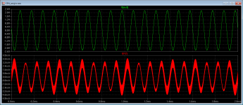
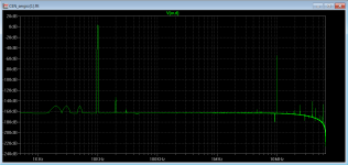
Another test with 4 current sources at the input, the 3 of the previous test and with the addicion of 10khz 6ma p-p (picture 3 and 4 )
Picture 1 is the fft at the output without the output filter capacitor , the IMD products are at -93dB
Picture 2 is the fft at the output with the output filter capacitor (2n2) , the IMD products are at -150dB
picture 3 is from the second test and is the input current and the output voltage with the output filter capacitor (2n2)
Picture 4 is the fft at the output with the output filter capacitor (2n2) and the 10khz signal.
In resume : the output filter capacitor in this type of circuit serves also for lowering the distortion caused by the intermodulation of the high frequency noise.
edit: this results are also valid for the original CEN designed by Patrick
Attachments
Last edited:
How about a low frequency (say <100Hz) switched capacitor power supply using low output capacitance solid state relays?
PS7901D-1A is 0.75pF typical 1.1pF max and good for 120mA continuous - enough to make a 60mA supply?
- Home
- Source & Line
- Digital Line Level
- Zen -> Cen -> Sen, evolution of a minimalistic IV Converter