arround the three I/V (I/U) converter topologies about
http://www.passdiy.com/pdf/Z-IV.pdf
there are a wide range of posts, and I am not able to read them all.
I have heard only various op amps like OPA637, AD829 and OPA827 against a normal resistor with follow high input impedance line amp so as the D1-topology. From my view the D1 topology sounds at best, follow from the "only one resistor" topology about
Digi Scoop 1
I/U converter that used op amps like the above mentioned still sound "over analytic" and a bit harsh like a tart wine.
The topology with jFETs so as various other discrete op amp solutions I have never heard.
Where can I find a description about the perceived audible differences between this various topologies?
Is there a clearly audible advantage by an I/U topology with jFET's - as described here - compare to the D1 I/U converter topology with IRF610 MOSFET's ?
Hi,
it´d be interesting to compare JFET-versions to bipolar versions.
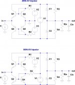
For parts of SEN-versions one could use the dual matched LSK389B (in my sims paralleling the transistors always resulted in higher THD-figures) or matched BF862 (if You can prevent them from oscillating). The BF862 would allow for a supply voltage as low as 9V for 2Vrms output signal.
What makes the bipolar versions interesting may be lower cost and easier to source parts, especially matched and complementary transistors, e.g the BC846/847 or BC847/857. They should require less supply current and lower supply voltage and allow for extreme compact building SMD circuits. THD-figures sim even better than the JFETs and they offer a decreased input impedance.
As a drawback, the bipolar versions of SEN-style need at least one additional voltage supply, referenced to gnd.
The ZEN-versions (or better CEN) need two supply voltages, referenced to gnd. But You´ll probabely need additional supplies anyway to power a buffer stage at the output.
jauu
Calvin
it´d be interesting to compare JFET-versions to bipolar versions.
For parts of SEN-versions one could use the dual matched LSK389B (in my sims paralleling the transistors always resulted in higher THD-figures) or matched BF862 (if You can prevent them from oscillating). The BF862 would allow for a supply voltage as low as 9V for 2Vrms output signal.
What makes the bipolar versions interesting may be lower cost and easier to source parts, especially matched and complementary transistors, e.g the BC846/847 or BC847/857. They should require less supply current and lower supply voltage and allow for extreme compact building SMD circuits. THD-figures sim even better than the JFETs and they offer a decreased input impedance.
As a drawback, the bipolar versions of SEN-style need at least one additional voltage supply, referenced to gnd.
The ZEN-versions (or better CEN) need two supply voltages, referenced to gnd. But You´ll probabely need additional supplies anyway to power a buffer stage at the output.
jauu
Calvin
Attachments
Last edited:
Yes, but there is only one way to find out -- build both and do AB test.Patrick
Correct. But dependent on the impressions from the other guys I'm either very curious and carried out an A/B test or I say, it is not worthwhile to investigate this exactly. Therefore the question.
If I build both now and the last case occurs, I've wasted a lot of time.
Last edited:
If I build both now and the last case occurs, I've wasted a lot of time.
Well diy is a hobby... If you are afraid of losing time by not building the best, you'll have to wait forever. There is always something new and exciting.
This was also one of my first ideas.
But it is a lot easier to make the first prototype with TO92 devices, and there are quite a few to choose from (K170, K369, K117, .....).
SOT23 devices are limited to a few, even though you can also get LSK170 in SOT23.
Also thermal management is easier with TO92, as the size of the PCB is dictated by the caps.
Maybe I'll do a BF862 version later in the end, when I get time.
For now, I can only offer to help you try this out.
Patrick
Hi,
I simmed the ZEN-style bipolar with:
+-2mA pp input current (as TIs PCM1795 and PCM1796)
BC847BS/BC857BS (spice models from Diodes) biased at 7.8mA
+12V supply
1k5 I/V-resistor + 220pF cap
Results:
V(out): 2.1Vrms
Total Harmonic Distortion (K2-K8): 0.000483% -106dB, clean spectrum
(even lower harmonics possible with increased supply voltage or differential output)
Noise (20Hz-20kHz): below 1µV (depends very much on the current source that is needed to null out centre currents of PCM-DACs)
Zin(dc): 65Ohms
Zin(ac): 2.65Ohms (and very linear into the MHz-range)
current output DACs like the PCMs show increasing THD when Zin is increasing above app. 20Ohms due to protection diodes
Vin, resulting from Zin: +-5.5mVpp
Zout: 1k5 || 220pF
upper Bandwidth limit: ~470kHz
TF: -1386mV/mA
I think thatare remarkable values for such a simple and tiny circuit that may be build from SMD-parts and less than 20x25mm PCB-size.
jauu
Calvin
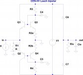
Incidentally this (what you called Zen Bipolar) is almost identical to the Leach 1999 circuit (2nd in the web page).
Except that he used 2 caps to replace your V2 & V3.
Moving Coil Cartridge Head Amps
Note that he did not ground the common emitter point of the mirror transistors (Q3, Q4).
Patrick
.
Except that he used 2 caps to replace your V2 & V3.
Moving Coil Cartridge Head Amps
Note that he did not ground the common emitter point of the mirror transistors (Q3, Q4).
Patrick
.
Last edited:
Hi,
had a look at the Leach circuit, which looks certainly similar at first glance.
There are a few points to remark though.
The Leach-pre is intended for usage with very low input currents and bias currents. In that topology the current mirroring Q3,Q4 ´steal´ some of the signal current, which means that not all the signal current swing can be used in the I/V conversion resistor. So either the output voltage is lower or one needs a larger resistor value. My sims showed losses of 10%-20% of outpt voltage.
Decreasing the currents through the collector-resisitors R3,4 is limited by the minimum needed base currents of Q1-Q4. The smaller idle currents through Q3,Q4 -compared to Q1,Q2- demand the use of the common emitter resistor R2 to allow for sufficient current in Q1,Q2. R2 should be two resistors with halfed values and referenced to Gnd (as sketched). Otherwise the input of the circuit will have no DC-reference point, because with a DAC-current output there is no input resistor R1, hence the input may find itself anywhere, but certainly not around 0V. Especially if You use DACs with centre currents like the PCM-series of TI. Without the gnd-reference via R1 Leach´s circuit would cease working as intended.
But there´s a subtle more to the gnd-referencing of the emitters of Q3 and Q4. If not referenced the input impedance -dc as well as as ac- nearly doubles against the ´referenced´ value.
Btw. the two 560k-resistors R1,R2 in EUVLs schematic serve a similar purpose...to reference and centre the circuit to gnd.
Leach´s circuit needs only one floating supply, but since the output impedance is rather high and the bandwidth and output voltage depend on the input impedance of the following device, a buffer stage would almost always be necessary. You can then use the power supplies of the buffer stage to supply the current mirror transistors. Breaking the current path through Q3,Q4 from the floating supply V1 lets all signal current pass through Riv. The output voltage is maximal and calculates to Riv times DAC-signal current.
jauu
Calvin
Attachments
Yes, but I would have to reach an age of more than a thousand years, to examine all my own and the other circuit ideas.Well diy is a hobby... If you are afraid of losing time by not building the best, you'll have to wait forever. There is always something new and exciting.
For this reason, I always need just a pre-selection with help of the experiences from other guys.
This leads me to the question, which frequency-dependent influence actually occurs through the three capacitances (input-, reverse- and D-S-capacitance) of the IRF MOS-FET from the Pass D1-Topology aboutHi, had a look at the Leach circuit, which looks certainly similar at first glance.
There are a few points to remark though.
The Leach-pre is intended for usage with very low input currents and bias currents. In that topology the current mirroring Q3,Q4 ´steal´ some of the signal current, which means that not all the signal current swing can be used in the I/V conversion resistor. So either the output voltage is lower or one needs a larger resistor value. My sims showed losses of 10%-20% of outpt voltage.
jauu Calvin
http://www.passdiy.com/pdf/Z-IV.pdf
(second drawing - simplified schematic D1).
Last edited:
There are 3 versions of the Leach circuit, Common Base (CB), Current Mirror (CM) and Common Emitter (CE).
Moving Coil Cartridge Head Amps
The one we simulated at the beginning was the CB and not the CM circuit (post #46).
I am the first to admit I know next to nothing about current mirrors and BJTs.
But I could not help wondering :
a) What would be the distortion like if the current mirror has some typical mismatch ?
(e.g. 50mV Vbe, 3% hfe, as in LS312/LS352 or SSM2210/2220)
b) What would be the PSRR of the circuit to noise in V2 & V3 ?
We did some very quick Spice simulations on (a) which revealed as much as 0.02% THD for 5% hfe mismatch !!
With the added components connected to Gnd (V2, V3, Q3, A4), the way the circuit functions has changed fundamentally (Please refer to my article for my interpretation). There is no longer a separate current loop for the DAC i_out through Riv back to Gnd. I am most concerned that the distortion spectrum would become more complex as a result.
I do very much look forward to your experimental results with real devices.
Patrick
PS My archive revealed quite a few BJT IV circuits based on current mirrors, e.g. the famous one from Jocko Homo.
http://www.diyaudio.com/forums/digital-source/6121-easy-build-i-v-stage.html
.
Last edited:
Hi,
while the so called "current mirror common base" stage of M. Leach certainly looks like its function relys on current mirror action, it is not what´s happening here. Usually the input and output of a C-M-stage is taken from the collectors. What we have here in fact is a complementary common base stage with temperature compensation. The difference to the common-base-stage of M.Leachs is in the biasing network. The diode connected Q3 and Q4 are used for temperature compensation and to set the idle currents of Q1 and Q2. This is maybe more obvious in Jocko´s circuit and the ZEN-I/V in #43. When dueal matched pairs are used for Q1,Q3 and Q2,Q4. input offset should not be an issue.
As Q3 and Q4 only serve as biasing devices -e.g dealing with DC working points, no AC- mismatches in Vbe and hfe should only lead to a slight variation of Input offset voltage (Q1,Q2s emitter potential, which ideally is 0V). With the biasing transistors Q3 and Q4 referenced to gnd and due to complementary action the input offset will be small already.
You could add a low-value pot between Q3 and Q4s emitters to null out dc-input-offset. Alternatively a dc-servo could feed the centre tap of two equal low ohmic resistors spanning between Q3 and Q4s emitters.
jauu
Calvin
If they are not current mirrors, perhaps you can explain why changing Q1 / Q4 hfe by 5% increases THD to 0.019%?
(in the CEN Bipolar as you posted in post #43)

There is also a factor of 5~10 more current from i_in not flowing through R-iv when compared to the JFET versions.
Namely it sinks directly to Gnd via the Gnd connection near V2 / V3 / Q3 / Q4.
The comparison was made under the same I/O conditons as yours (2mA input current, R-iv 1.5k).
I am sure you can repeat the results, since we built a Spice model according to your schematics to repeat your results in post #49 first.
When we have some more time, we'll try to find out about PSRR to V2 & V3.
Patrick
.
(in the CEN Bipolar as you posted in post #43)
There is also a factor of 5~10 more current from i_in not flowing through R-iv when compared to the JFET versions.
Namely it sinks directly to Gnd via the Gnd connection near V2 / V3 / Q3 / Q4.
The comparison was made under the same I/O conditons as yours (2mA input current, R-iv 1.5k).
I am sure you can repeat the results, since we built a Spice model according to your schematics to repeat your results in post #49 first.
When we have some more time, we'll try to find out about PSRR to V2 & V3.
Patrick
.
Last edited:
- Home
- Source & Line
- Digital Line Level
- Zen -> Cen -> Sen, evolution of a minimalistic IV Converter