I foresee a heap of questions related to a certain new, cheaply designed ES9018 board, one that looks cheap on the surface, but once filled with parts; not so much. its hard to tell, it appears to be a single layer PCB with a very basic power supply, no controller and very basic opamp IV stage..... the amount of time and money and hack jobs needed to make it function well, will far outweigh any initial price difference.
those looking at a cheaper ESS dac that suits the fifo may look at the AKD16 ($50), which uses an ES9016 dac, has u.fl connector for MCK, has w.fl connectors for the rest of the inputs and has a proper compact PCB layout with segmented power and ground planes.
w.fl sockets can easily be soldered in the u.fl positions on the fifo clock board, thats what I do with its bigger brothers the AKD12P
Last edited:
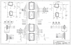
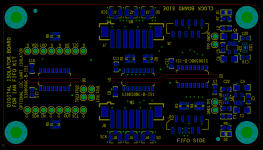
FIFO isolator board V2.0
1. Making it easier to assemble the resistor arrays.
2. 16-SOICN package ICs on top for better layout.
3. Including optional LP5900 LDOs.
4. Making SI8606 as optional I2C/UART isolator.
5. Including two power LEDs to indicate power good on both side.
Function and interface compatible with V1.0
Ian
1. Making it easier to assemble the resistor arrays.
2. 16-SOICN package ICs on top for better layout.
3. Including optional LP5900 LDOs.
4. Making SI8606 as optional I2C/UART isolator.
5. Including two power LEDs to indicate power good on both side.
Function and interface compatible with V1.0
Ian
Attachments
Very nice Ian! I'm in for building a couple if/when you make protos available. Btw, Happy New Years!
Thanks MisterRogers, Happy New Year to you too.
Ian
nice work Ian! so U9 and U10 are TPS7A style DFN package regs? I just ordered some of these including the negative counterparts TPS7A3001 for my portable dac, I will be using them with a simple mosfet follower for higher current to power the buffers for added transient response.
I foresee a heap of questions related to a certain new, cheaply designed ES9018 board, one that looks cheap on the surface, but once filled with parts; not so much. its hard to tell, it appears to be a single layer PCB with a very basic power supply, no controller and very basic opamp IV stage..... the amount of time and money and hack jobs needed to make it function well, will far outweigh any initial price difference.
those looking at a cheaper ESS dac that suits the fifo may look at the AKD16 ($50), which uses an ES9016 dac, has u.fl connector for MCK, has w.fl connectors for the rest of the inputs and has a proper compact PCB layout with segmented power and ground planes.
w.fl sockets can easily be soldered in the u.fl positions on the fifo clock board, thats what I do with its bigger brothers the AKD12P
So qusp, you run the Ian fifo with the AKD12P?
/
nice work Ian! so U9 and U10 are TPS7A style DFN package regs? I just ordered some of these including the negative counterparts TPS7A3001 for my portable dac, I will be using them with a simple mosfet follower for higher current to power the buffers for added transient response.
Yes, the package is LLP-6, actually it's DFN.
LP5900SDX-3.3/NOPBCT-ND
http://www.digikey.ca/product-detail/en/LP5900SDX-3.3/NOPB/LP5900SDX-3.3/NOPBCT-ND/3527159
Ian
Cool OK, well OK if you have rework station =)
my mistake, the TPS7A3001 (Neg) and TPS7A4901 (Pos) are 8 lead DGN capable of up to - and + 36vdc 150mA/200mA. they are like MSOP-8 with powerpad and very low noise, not as good as the TPS7A4700 but only about double the noise of that @ 13µVRMS. but and this is a big but, they come in matching positive and negative in the same small package, annoyingly rare that is these days to find a +/- pair from the same range/package.
I guess they just expect everything to be running a charge pump to generate the midsupply instead of running a dual rail supply. its literally the only matching low noise LDO pair I know of, there is the LT3032 which is a bipolar reg in a single package at 30µV noise but everything else is all positive, or there is a negative part in a completely different package with completely different specs
Hi,
I have spent the last 4 days reading through this 1800 post thread and I have not found an answer to my questions. I'd appreciate if someone could help me find answers to my questions below -
1. How exactly does the reclocking of the outgoing high quality clock work ? There's some flip flop in use but I cant understand its operation for this purpose. The "documentation" is mostly about the kit and doesn't really go into details about the schematic or code or anything. Where can I find implementation details like these ?
2. Does anyone have any real world spdif jitter measurements comparing this to a typical clock recovery device like the WM8804/5 ? Like say compare the jitter of the I2S output when a mass market cd/dvd/bluray player is hooked up to a WM8805 v/s this fifo.
3. Same as above, except subjective impressions instead of objective measurements. Sound quality experience when you have this fifo instead of a WM8804/5.(ofcourse with everything else in the playback chain constant).
Thanks.
WM8804 has roughly 20x the RMS jitter (actually i'm being generous to the wolfson there)
tbh if you havent worked out how it works by knowing there are flipflops and a high quality clock on the output of some memory, i'm not sure how I can make that any clearer. the output clock jitter plus the flipflop/clock buffer jitter is the sum total of the output jitter, so its posible to have less than 1ps output jitter
nobody is going to explain or detail the software or hardware further than is already in this thread.
nobody is going to post a schematic, besides theres a lot going on inside the fpga too, you want source code?
what specifically dont you understand?
also the wolfson isnt a clock recovery part, thats why its got lower jitter (~50ps RMS jitter) than the others that do use the recovered clock.
Last edited:
take a look at this link
Synchronous Reclocking? H i F i D U I N O
the best way anyway..
MCLK from an ultra low phase noise XO, reclocking the BCK with same MCLK
All synchronous
Synchronous Reclocking? H i F i D U I N O
the best way anyway..
MCLK from an ultra low phase noise XO, reclocking the BCK with same MCLK
All synchronous
Last edited:
.. by knowing there are flipflops and a high quality clock on the output of some memory...
what specifically dont you understand?
basically what is is that happens, and how, that makes sure the memory doesn't ovrflow or dry out ? There's no pll, doesn't seem to be vcxo or anything so what controls the outgoing clock ?
also the wolfson isnt a clock recovery part, thats why its got lower jitter (~50ps RMS jitter) than the others that do use the recovered clock.
I am not sure what you mean. Isn't that the whole idea of a spdif receiver ?
Andrea, thanks for the link. I think the "How it works" part of it might have the answer to my question.
fifo memory is large by normal scale and it empties to half full between tracks to avoid under/over-run
doesnt seem to be an XO? are you sure you are looking at the same design? the output board comes in 3 flavors, the single clock board that comes standard and contains the clock buffer/s and 2 sets of 3 flip-flops, the dual clock board which has the same but with 2 clocks and the si570 multispeed DSPLL clock generator which will provide clock multiples for anything from 44.1->384kHz.
all of them take the output of the fifo memory buffer/fpga and reclock it (with or without galvanic isolation inbetween) and output MCLK plus bck, lrck, sdata all clocked from the same clock and this is then optionally fed synchronously to the dac chip.
the flip-flops are clocked by the output clock
its impossible to believe you read or even searched the thread for this information and didnt find it; this project/product and its development has been well documented and discussed here, much better than most other projects. there is not, nor will there ever be source code or full schematics posted, nor should it be expected, sorry but that question itself tends to put me a bit offside.
its not a complex concept, but rather an old one executed with more modern, high quality and appropriate technologies. it is then supplied on a very skilled high speed impedance controlled layout with appropriate connectors.
re WM8804/5
from the datasheet
The goal here is to synchronize a clock generated from a PLL and high quality oscillator to incoming S/PDIF data stream. This is different to usual approach of using a PLL to recover a clock from the S/PDIF data stream, which inherently has to track the jitter to maintain lock.
Last edited:
fifo memory is large by normal scale and it empties to half full between tracks to avoid under/over-run
And how does it deal with gapless/streaming? I think one of the main questions percy has is about the avoidance of under/over-run when dealing with 2 isolated clock domains.
I know what he means, it depends on how crappy the clock in the source is and it is never a problem with the spdif input as he seems to be interested in. i'm yet to have a problem, even with streaming there are often momentary gaps, adds etc and gapless is very rarely a single file, just a number that run into each other seamlessly (which still provides an opportunity to adjust). the time needed to fill/empty the buffer seems to be very large with the normal quality of input clock. this 'problem' has been discussed a number of times already in this thread, its a non-issue, just something for people to talk about or for other competitors to mention in an effort to criticize, but does not present in the wild.
Ian has said that the memory is fast enough that it could empty in between samples if needed, but its simply hasnt been needed. it has been talked about, but it seems not a single person has ever experienced it
Ian has said that the memory is fast enough that it could empty in between samples if needed, but its simply hasnt been needed. it has been talked about, but it seems not a single person has ever experienced it
Last edited:
Andrea, thanks for the link. I think the "How it works" part of it might have the answer to my question.
translated for the FIFO board (to get the lowest jitter): a really low jitter master clock (phase noise at least -125dbc@10Hz) as the FIFO master clock, do not take BCK from FIFO board but take it re-clocked/divided from the MCLK, and feed directly the DAC chip.
The final I2s signal will be isolated from the source jitter, and FPGA jitter will not affect the BCK. The goal is to keep the BCK as clean as possible.
eg. for those who run the TDA1541 in NOS mode: master clock at 11.2896 MHz to the FIFO board, WS and DATA from the FIFO board to the DAC chip (supposed to be already clean), master clock divided by 4 to DAC chip BCK.
The same way could be used for any other DAC chip, OS or NOS
IMHO obviously, the best solution.
I know what he means, it depends on how crappy the clock in the source is and it is never a problem with the spdif input as he seems to be interested in.
I agree that it probably isn't a problem in most cases, but you could have a case where the source clock is extremely stable and jitter-free, but simply runs too fast or slow in an absolute sense - so you will always be fighting the theoretically hard-to-solve issue of trying to match two non-matching time domains, unless you have a "rate feedback" mechanism (like async USB). With S/PDIF you either end up doing "cut and paste" by discarding or filling in quiet parts, or with a sample rate converter.
I am not trying to criticize Ian's design, I am merely pointing out, for purposes of clarity, a structural issue faced by any system lacking an end-to-end synchronisation feedback loop. Blame the designers of S/PDIF etc...
- Home
- Source & Line
- Digital Line Level
- Asynchronous I2S FIFO project, an ultimate weapon to fight the jitter