HDMI? not going to happen, licensing rules it out for hobbiest projects.
multichannel? welcome to the line of people poking Ian with a stick
I surrender
I don't think multichannel FIFO gonna be any problem. But I'm still struggling with the DSD mute pattern which will be part of the FPGA logic. Anybody has idea?
Ian
My new digital source will be based on a high end USB/I2S board followed by a digital filter and PCM1704 dacs. There will be a dual freq. very low jitter clock that will feed everything, synchronously.
Digital filter chosen requires reclocking on outputs and idea is to use simple and well implemented d-type flip-flops.
I'd like to know if the FIFO board might be better than flip-flops solution.
I'm not sure this could be a good idea as the USB board already performs a digital buffering and its I2S output already have a very good quality, with the right clock.
Suggestions and thoughts? Thanks!
HI fvale, in theory a fifo integrated directly in the DAC chip and operated with a high precision clock near would be the first method to reduce jitter to mininal, the second best and more pratical method is the design you see described in this thread. Many HI-end DAC integrate some jitter reduction mecanism but to my knowledge they are still not immune to the jitter of the source. So a simple answer would be yes in theory ;-) in pratice I will recevied my FIFO in a few hours and will do a comparaison with some HI-END commercial USB interface.
I hope you have good clocks for the fifo in this comparison? without good clock you will not get best results. fifo is all about preparing best conditions to get the best out of your clocks, leaving you with little more jitter than the clock itself+clock buffer
fvale: you cannot feed pcm1704 directly with fifo unless you have the new PCM convertor board, the 1704 requires specialist PCM reclocking, firstly its mono, but it also has other peculiarities.
fvale: you cannot feed pcm1704 directly with fifo unless you have the new PCM convertor board, the 1704 requires specialist PCM reclocking, firstly its mono, but it also has other peculiarities.
Yes, I know that 1704 doesn't accept I2S signals, the PMD200 filter I, and a expert friend of mine, will use has left justified output.
Anyway now we're focused in finding the optimal best methode to reclock digital filter outputs; being a DSP reclocking is not optional, unfortunately
Anyway now we're focused in finding the optimal best methode to reclock digital filter outputs; being a DSP reclocking is not optional, unfortunately
Yes, I know that 1704 doesn't accept I2S signals, the PMD200 filter I, and a expert friend of mine, will use has left justified output.
Anyway now we're focused in finding the optimal best methode to reclock digital filter outputs; being a DSP reclocking is not optional, unfortunately
the PMD200 is completely outgunned by Fifo plus the reclocker I linked above that Ian designed to work with fifo to enable working with various dacs that dont do i2s
Welcome to the line of people poking Ian with a stick
I think you need a bigger stick
My new digital source will be based on a high end USB/I2S board followed by a digital filter and PCM1704 dacs. There will be a dual freq. very low jitter clock that will feed everything, synchronously.
Digital filter chosen requires reclocking on outputs and idea is to use simple and well implemented d-type flip-flops.
I'd like to know if the FIFO board might be better than flip-flops solution.
I'm not sure this could be a good idea as the USB board already performs a digital buffering and its I2S output already have a very good quality, with the right clock.
Suggestions and thoughts? Thanks!
Hi fvale,
The goal of a I2S fifo is to isolate the the clock domain from the I2S source and replace it with a better secondary clock. I don't know what high end USB you gonna use? But if the clock from your USB source is good enough then I don't think you need a fifo. So, to use or not to use a fifo is totally up to the clock quality of your i2s source
.Regards,
Ian
I think you need a bigger stick
no, a small stick is fine, i'm only politely (but reasonably regularly) poking with the stick, because I know that my (and your) agenda isnt really Ian's agenda, since at least for now hes 2 channel only.
I didnt mention it, but either your skimming is not very good, or you didnt really skim the whole thread, its been mentioned many times, not just by me.
Hi fvale,
The goal of a I2S fifo is to isolate the the clock domain from the I2S source and replace it with a better secondary clock. I don't know what high end USB you gonna use? But if the clock from your USB source is good enough then I don't think you need a fifo. So, to use or not to use a fifo is totally up to the clock quality of your i2s source
Regards,
Ian
Interesting information Ian, many thanks. I will use this USB board: USB Audio interface | ABC PCB
Maybe not exactly developed for diy use, but it's available to anyone.
Oscillators on board should be fine, anyway there's the possibility to bypass them and enter with a master clock. Company already has low jitter external clocks of single frequency, but they told me that soon they'll have a dual frequency master clock.
I will use a external master clock to feed everything.
Problem in this usb dac project is to choose best way to reclock signals OUT of the Pacific Microsonics digital filter. As far as I can read around, beeing DSP based, reclocking at its outputs is NOT optional!
Last edited:
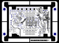
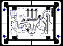
Si570 clock board PCB V3.0
Here is the Si570 clock board V3.0 PCB design. There were 2 previous versions, V1.0 and V2.0. None of them could become the finial.
Onboard LDO removed completely to make good use of external low noise high performance power supply, or battery directly. With on board LDO limitation removed, power supply selection becomes more flexible, different PSU solutions could be put into evaluation and then to decide according to actual sound quality and personal preference. More PCB space left that can be used for enhanced bypass capacitors, EMI filters and possible XO shield can. Layout design with better RF performance gains from the PCB space as well to meet the MCLK closing to 100MHz(based on less than 1ns actual clock raising/falling time, the frequency range could be extended at least more than 5 times which is 500MHz).
Inverted MCLK was implemented as the default clock phase according to ESS APN recommendation and actual listing test. But it could be disabled for further more evaluations.
An UART port was included on PCB for potential thirty party external controllers. Protocol has already been supported by the ATMeaga8 Si570 driver. UART isolator is highly recommended for connecting with the external controller if your clock board has already been isolated from the FIFO.
Most of the features we have discussed before are also included in this V3.0 design. I’ll order the PCB prototypes once again. Just hope it could be the last version before the Si570 GB.
Ian
Attachments
Your productivity never ceases to amaze me Ian!
Thanks MisterRogers, I know you have been waiting for this littlt clock board for too long. I'm just concerned about the design is not perfect, that's why it's been revised for three times...
Have a nice holiday.
Ian
what amazes me is how consistently clean you manage to get with high speed designs on 2 layer PCBs....
great skill indeed
thanks...
Both double layer and multi-layer PCB could be excellent design if we take impedance control into account. However if there is no enough space to place wider clock traces on PCB, then we have to use multi-layer, like some ESS9018 DAC.
Ian
Both double layer and multi-layer PCB could be excellent design if we take impedance control into account. However if there is no enough space to place wider clock traces on PCB, then we have to use multi-layer, like some ESS9018 DAC.
Ian
Ian, do you use formulas to calculate trace impedance when laying out this and similar boards?
Ian, do you use formulas to calculate trace impedance when laying out this and similar boards?
Hi Aos,
Yes, I do calculation but not use formulas. Design software can do calculating and simulation for the PCB designs on trace impedance control in SI section, like Cadence Allegro.
Some on-line calculators also work, as:
Edge Coupled Microstrip Impedance | Electrical Engineering Tools | EEWeb
Microstrip Transmission Line Characteristic Impedance VB Script Calculator Using a Formula by Brian C Wadell
Regards,
Ian
- Home
- Source & Line
- Digital Line Level
- Asynchronous I2S FIFO project, an ultimate weapon to fight the jitter