Hi,
I have tried "double speed mode" with async FIFO + dual XO board (and Buffalo2), using recently purchased 45mhz and 49mhz cchd-957.
modifying was quite easy, except mounting cchd-957 because I didn't have suitable adopter board.
Tested playing 352.8khz music (from 2L trial download) and 384khz test track (from MSB website).
both were played fine with bypassing OSF mode of ES9018.
Great!
Hi Ian
I need a couple of PCB for my dual clock board, but I can't find any information in the GB.
Will post later
Ian
Hi,
I have tried "double speed mode" with async FIFO + dual XO board (and Buffalo2), using recently purchased 45mhz and 49mhz cchd-957.
modifying was quite easy, except mounting cchd-957 because I didn't have suitable adopter board.
Tested playing 352.8khz music (from 2L trial download) and 384khz test track (from MSB website).
both were played fine with bypassing OSF mode of ES9018.
Great!
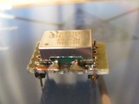
This is my ugly XO adopter board.
Good to know that. I'll try the 3XXkhz later. Will supply the good XO adapter KIT for sure together with GBII. Your XOs will look nicer.
What the difference between OSF/bypass ?
Ian
I have tried OSF bypass before too and i'm not quite sure about the results, I believe its one of the ess strengths, the filters seem very well handled despite not being linear phase. I think by running synch AND OSF bypass you are making it just like any other high performance dac
When playing 352.8k files, I never felt OSF mode is necessary. Hard to decide which is better for me between OSF mode and bypassing OSF mode.
With lower SR recordings, high frequencies are more natural with OSF mode.
Especially when playing 16/44.1k materials I never bypass it.
These are my subjective opinion and might differ with different post filter designs.
With lower SR recordings, high frequencies are more natural with OSF mode.
Especially when playing 16/44.1k materials I never bypass it.
These are my subjective opinion and might differ with different post filter designs.
I2S to PCM convertor daughter board PCB design
Hi Vzs, Hi Zinsula
Are you there?
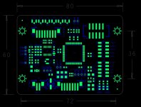
The I2S to PCM convertor daughter board got some progress. The PCB layout alos finished. All dimensions are as same as the clock board and could be stacked together. Please see the attached pictures for details and let me know for your suggestions.
I don't think it could catch up with the GB II. But I hope I can order the prototype PCB together with GB II.
Regards,
Ian
Hi Vzs, Hi Zinsula
Are you there?
The I2S to PCM convertor daughter board got some progress. The PCB layout alos finished. All dimensions are as same as the clock board and could be stacked together. Please see the attached pictures for details and let me know for your suggestions.
I don't think it could catch up with the GB II. But I hope I can order the prototype PCB together with GB II.
Regards,
Ian
Attachments
Yes![...]Are you there?[...]
I didn't feel to ask you about that additional board, as you seem to have already enough work right now.
From the picture, not everything is clear to me...
- What is J5 for?
- I assume U5 is a D-FlipFlop, do you reclock all 6 lines with this? As DATA lines should be quiet during conversion, this might be OK, on the other hand, reclocking CLK and LLLR with separate single (and properly decoupled) FlipFlops (picogates) would make sure those lines are less influenced from each other.
-J7, it would be good if you can put DR and DRn, and DL and DLn as pairs. These pairs of data are kind of a balanced signal (complementary) and small loops are beneficial, also helps the layout on the DAC board.
It would be good to have something like this:
GND-CLK-GND-LLLR-GND-DLn-DL-GND-DR-DRn
Those using only DL and DR still would have a GND cable in between. A 10 pin connector would be needed though...
- I assume you did it already with U3 and U4 but not sure: Good deecoupling of U1 and U5. U5 is critical for performance and should get very clean power.
Thank you anyway! Ciao
Hi Ian, Zinsula!
Nice to see progress with this board.
- I'm sorry but I feel that your specialized knowledge in this respect is beyond mine so I subscribe to the remarks posted by Zinsula for both dedicated flip-flops and the extended header.
Good decoupling is indeed a must, although the image is not very clear it seems you have U4 for the flip-flop U5 and U3 for the FPGA U1.
- The 16bit word length is the default that's why there is no jumper for it?
Thank you!
Zsolt
btw. J5 is probably the JTAG header to program the fpga.
Yes!
I didn't feel to ask you about that additional board, as you seem to have already enough work right now.
From the picture, not everything is clear to me...
- What is J5 for?
- I assume U5 is a D-FlipFlop, do you reclock all 6 lines with this? As DATA lines should be quiet during conversion, this might be OK, on the other hand, reclocking CLK and LLLR with separate single (and properly decoupled) FlipFlops (picogates) would make sure those lines are less influenced from each other.
-J7, it would be good if you can put DR and DRn, and DL and DLn as pairs. These pairs of data are kind of a balanced signal (complementary) and small loops are beneficial, also helps the layout on the DAC board.
It would be good to have something like this:
GND-CLK-GND-LLLR-GND-DLn-DL-GND-DR-DRn
Those using only DL and DR still would have a GND cable in between. A 10 pin connector would be needed though...
- I assume you did it already with U3 and U4 but not sure: Good deecoupling of U1 and U5. U5 is critical for performance and should get very clean power.
Thank you anyway! Ciao
Hi Ian, Zinsula!
Nice to see progress with this board.
- I'm sorry but I feel that your specialized knowledge in this respect is beyond mine so I subscribe to the remarks posted by Zinsula for both dedicated flip-flops and the extended header.
Good decoupling is indeed a must, although the image is not very clear it seems you have U4 for the flip-flop U5 and U3 for the FPGA U1.
- The 16bit word length is the default that's why there is no jumper for it?
Thank you!
Zsolt
btw. J5 is probably the JTAG header to program the fpga.
Very good points. I'll show you a more clear layout picture this evening.
Ian
Yes!
I didn't feel to ask you about that additional board, as you seem to have already enough work right now.
From the picture, not everything is clear to me...
- What is J5 for?
- I assume U5 is a D-FlipFlop, do you reclock all 6 lines with this? As DATA lines should be quiet during conversion, this might be OK, on the other hand, reclocking CLK and LLLR with separate single (and properly decoupled) FlipFlops (picogates) would make sure those lines are less influenced from each other.
-J7, it would be good if you can put DR and DRn, and DL and DLn as pairs. These pairs of data are kind of a balanced signal (complementary) and small loops are beneficial, also helps the layout on the DAC board.
It would be good to have something like this:
GND-CLK-GND-LLLR-GND-DLn-DL-GND-DR-DRn
Those using only DL and DR still would have a GND cable in between. A 10 pin connector would be needed though...
- I assume you did it already with U3 and U4 but not sure: Good deecoupling of U1 and U5. U5 is critical for performance and should get very clean power.
Thank you anyway! Ciao
Hi Ian, Zinsula!
Nice to see progress with this board.
- I'm sorry but I feel that your specialized knowledge in this respect is beyond mine so I subscribe to the remarks posted by Zinsula for both dedicated flip-flops and the extended header.
Good decoupling is indeed a must, although the image is not very clear it seems you have U4 for the flip-flop U5 and U3 for the FPGA U1.
- The 16bit word length is the default that's why there is no jumper for it?
Thank you!
Zsolt
btw. J5 is probably the JTAG header to program the fpga.
Hi zinsula, Hi Zsolt
Thank you for your very good comments!
1, Right, J5 is the JATEG port of the FPGA;
2, U5 is the Patato GHzTTL flip-flops, that is the fastest flip-flop I could find and have to use so far because those legacy PCM DACs do not accept MCLK.Actually data signals do not need to be re-clocked. But to align them with falling edge of CLK, we have to do that. The good thing is they don't have same effective edge. It also has an independent power supply with low noise LDO and enhanced decoupling and filtering network. And futher more, that LDO could be bypassed by replacing it with customized PSU or even batteries into TP4,TP5 and TP6 to achieve better performance.
3, J7 use to be CLK-GND-LLLR-GND-DL-DR-DLn-DRn. But your suggestion makes more sense. Now I already changed them to GND-CLK-GND-LLLR-GND-DLn-DL-GND-DR-DRn with PH2.0 10P connector. Each of those PCM output signals comes with an optional U.FP socket position just in case they required by some applications.
4, Yes, the FPGA also has an independent low noise LDO, but just regular decoupling.
5, Yes, no jumper is the 16bit, but I suspect few people use it. So, in most of the cases, there should be only one jumper selecting the data length.
I attached the revised PCB layout in a more clear picture. Please let me know for any comment.
Have a good night.
Ian
Attachments
Hi Ian,
One of these days I read Pedja's Aya DAC rev2 manual and beside that its a great learning document what caught my eyes is his care about treating digital signal as analog - I mean trying to avoid common/shared return paths or make them as short as possible.
- You have also created two "islands" one for the FPGA and for the flip-flops, which is very good, however I would move U1 as far to the right as possible, letting more ground plane between U1 and U5.
- In order to have shorter-common return paths it would be nice to have DC input also more to the right - but I see this is hardly possible - maybe if you move C26 up and J6 in its place.
Hope these makes sense.
Thank you!
Zsolt
Hi Ian,
One of these days I read Pedja's Aya DAC rev2 manual and beside that its a great learning document what caught my eyes is his care about treating digital signal as analog - I mean trying to avoid common/shared return paths or make them as short as possible.
- You have also created two "islands" one for the FPGA and for the flip-flops, which is very good, however I would move U1 as far to the right as possible, letting more ground plane between U1 and U5.
- In order to have shorter-common return paths it would be nice to have DC input also more to the right - but I see this is hardly possible - maybe if you move C26 up and J6 in its place.
Hope these makes sense.
Thank you!
Zsolt
Thanks Zsolt,
Another good point. I think I can move U1 more to the right to leave more GND space between U5. But to stack the daughter board over the clock board, I have to keep the DC input port J6 in that position which is corresponding to the DC output on the FIFO board. However I could separate part of the ground plan in between to recude the common return path.
Have a nice weekend.
Ian
Are you going to have ground and vcc planes on this board or just a two layer design?
Having a contigous ground and power planes would provide the best returns for the digital signals, as the best return path for the digital signals is an unbroken plane directly under the signal, and preferably ground, thouh an unbroken power plane provides a good retyrn path as well.
Digital signals should be treated as and routed as digital, there is plent of info covering digital PCB design.
Last edited:
I have now, they are nice designs,
The offer still stand on the info, I have a LOT of info regarding PCB design and especially high speed layout and decoupling that I have collected over the years, should have some new interesting stuff soon as I'm going on a training session looking at new software for Power Deliver System simulation which should be interesting.
The offer still stand on the info, I have a LOT of info regarding PCB design and especially high speed layout and decoupling that I have collected over the years, should have some new interesting stuff soon as I'm going on a training session looking at new software for Power Deliver System simulation which should be interesting.
Last edited:
indeed they are and they incorporate many of the things you and I have found lacking in other designs here in the past. proper i2s termination, use of differential ZIF and u.fl connections for critical path, everything well decoupled for DC and AC locally etc.
nice extras as well, vibration mounts, LED indication at all points in the signal flow to illustrate/indicate correct operation. small SMD pfc protection, the use of kemet 4 terminal CLC and CRC parts. ticks all the boxes for me, well if only it were blue teflon to match my dac =D
that being said, i'm sure Ian appreciates the feedback and thanks for popping in
@Ian: marce knows his **** for high speed multilayer layout, that short post above is good indication youre on the right track
Last edited:
Are you going to have ground and vcc planes on this board or just a two layer design?
Having a contigous ground and power planes would provide the best returns for the digital signals, as the best return path for the digital signals is an unbroken plane directly under the signal, and preferably ground, thouh an unbroken power plane provides a good retyrn path as well.
Digital signals should be treated as and routed as digital, there is plent of info covering digital PCB design.
I have now, they are nice designs,
The offer still stand on the info, I have a LOT of info regarding PCB design and especially high speed layout and decoupling that I have collected over the years, should have some new interesting stuff soon as I'm going on a training session looking at new software for Power Deliver System simulation which should be interesting.
Hi Marce,
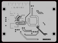
Thank you for your comments. Good to know you are a high-speed PCB design expert. The attached lauout is the ground plane of this small daughter board. I'm trying to make it as a whole GND piece and make the returing path as short as possible. All the clock output socket connect to the ground plane right under the pads. All the returing path to the bypass caps are within 1 inch, as well as to the regs. I just don't have time doing the simulation. Actually only the U5, the flip-flop decide the performace. FPGA has nothing to do with the output jitter. The void on the GND plane is for eliminate the common returning path, althrough it couldn't be 100% removed
. To reduce the high frq noise come from the DC power, I include the NFM EMI filer, different from the normal MLCC, NFM could still keep good suppression performance up to a couple of GHz.
Please let me know for any suggestion.
Thanks again,
Ian
Attachments
- Home
- Source & Line
- Digital Line Level
- Asynchronous I2S FIFO project, an ultimate weapon to fight the jitter