I've seen the datasheet, 2.1168 x n.
Spdif in not the best solution, I2S is definitely a cleaner solution, but if no other solution I'll use spdif.
Well, I'm waiting for Ian impression about this.
Hi Andrea,
In the above post, I'v already confirmed you can feed I2S signals directly from CDPro into FIFO.
") . My FIFO could handle I2S with sck running at 48*fs.
. My FIFO could handle I2S with sck running at 48*fs.Regards,
Thank you for your response, impressive.[...]Any word length between true 16bit to true 32bit is working[...]
Actually you wrote this in the manual IanI2SFIFOV1.0.pdf at I2S input: "44.1 KHz, 48 KHz, 88.2 KHz, 96 KHz, 176.4 KHz, 192 KHz - 16bit, 24bit or 32bit" but I thought these are data bits not word lengths.
Hi Ian,
It looks promising. I also have some remarks:
Five jumper selectors
- it seems that beside jmpstopclk you used negative logic to set their function
- according to the simulations they look correct, but this negative/positive logic mixing is a bit confusing. Would be nice to be consistent and use either negative or positive logic for all
Data and clock lines for all three images
- is confusing that the MSB of the right channel starts with 0 while the MSB of the left channel with 1; so it looks like they are delayed by one clock, but probably not
- for stopped clock mode I also count +1 clock but I don't think this is an issue since only the last X bits will be transferred to the parallel DAC registers (after latch has gone low)
Concerning reclocking I share zinsula's opinion from #388.
A suggestion about board layout: it would be nice to be stack-able above the clock board - probably same size. If it's input would come from the FIFO board then the input connector could be in same position as on the clock board.
Thanks, Zsolt
Thing about it is both PMD100 and SM5842 were typically fed from a CS8412 with Mo=0, m1=1, M2=0, M4=0, which is phillips I2S. I don't remember there being issues.
If the next Fifo is going to offer Sony format, why not offer splitting the data into left and right as well, and shifting registers for different bitdepths.
If it could be flexible enough to plug directly into a pair of PCM1704, PCM56,or AD1865, it would be a huge boon to the whole NOS scene.
Also if we could plug in the Fifo to a pair of PCM1704's at 352.8 we could start making our own 8x oversampling algorthms with the computer.
As far as upgrading the 11289.6 clock on the standard Fifo, I think the Tent €24,37 XO-DIY, is the only option. There seems to be no 256fs clocks on the market that will run at 3.3V.
Hi, Ian
Your FIFO+reclocker combined with Sabre dac is really impressive, especially when synchronous mode between the dac and reclocker.
When I first fired up SDTrans384 - FIFO plus reclocker( U1 is replaced with NDK NZ2520SD ) - Buffalo2 setup, I immediately noticed this obviously outperforms SDTrans384 - Buffalo2 combo.
Side by side comparison was never needed.
Now I can hear more low-level informations more easily and feel as if near the everything some more precise - bass are better controlled, less harsh Hi, and so on.
Really good job indeed, and I'm glad to see you still seek more improvement and versatility...
Thanks!
Hi wktk_smile,
You are the first guy who implements the integration of FIFO and Sabre32 DAC( or Buffalo) I know so far. Especially running it at synchronized mode. Congratulations! I suspect a lot of people are waiting for this good news.
Thank you so much for sharing your experience. I'm very interested in your hookups. Could you please let us know a bit more details? or some pictures? With the synchronized mode, what frequency of your NDK XO did you use? Actually the Buffalo III I bought just arrived yesterday. Hopefully I could try it next week. I have to focus on upgrading the FIFO and design the new PCM daughter board now.
Regards,
You can fed I2S into PMD100 or SM5842 but you will loose the LSB and the left/right channels will be reversed. I've done thatThing about it is both PMD100 and SM5842 were typically fed from a CS8412 with Mo=0, m1=1, M2=0, M4=0, which is phillips I2S. I don't remember there being issues.
accidentally so I know. CS8412 supports the right justified format for 16bit or 18bit (no.5 and 6) which is indeed a correct format for both PMD100 and SM5842. I'm using CS8414 with AD1865 in NOS mode so I've sweat on these manuals a lot The converter board Ian is preparing will support several output formats, including for those DACs you mentioned and the Left Justified format for the digital filters which don't support I2S.
Last edited:
Hi wktk_smile,
Thank you so much for sharing your experience. I'm very interested in your hookups. Could you please let us know a bit more details? or some pictures? With the synchronized mode, what frequency of your NDK XO did you use? Actually the Buffalo III I bought just arrived yesterday. Hopefully I could try it next week. I have to focus on upgrading the FIFO and design the new PCM daughter board now.
Regards,
XO is NZ2520SD-22.579200M-NSA3449C, and later I also replaced U2 with 24.576mhz one.
they are not fast as ES9018's MCLK, but fine for actual use for playing up to
96khz pcm. While playing 176.4khz and 192khz, bypassing OSF mode was required.
Attachments
XO is NZ2520SD-22.579200M-NSA3449C, and later I also replaced U2 with 24.576mhz one.
they are not fast as ES9018's MCLK, but fine for actual use for playing up to
96khz pcm. While playing 176.4khz and 192khz, bypassing OSF mode was required.
Hi wktk_smile,
Thank you for the pictures. Very impressed.
Actually, the dual clock board has a reserved double speed mode which could run 45.xxxx and 49.xxxx MHz XO for ES9018 or Buffalo DAC to make us more happy, especially for the synchronized mode. I'll publish the setting document after I conformed that on a real Buffalo III dac. Maybe I still need to inquire you when I go the hookup.
Although stock XOs may be "generic" ones, I felt they are not bad.
Even with stock XO, FIFOboard + reclocker gives good results.
Yes, at least that is the original clock from a crystal, don't need to trace another input clock.
Have a nice weekend.
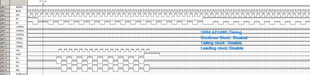
New I2S to PCM converter board design in synchronize mode
Hi Zsolit, Hi Vzs,
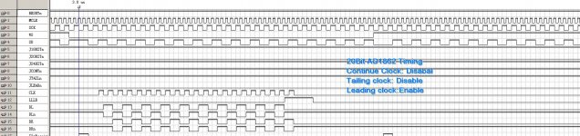
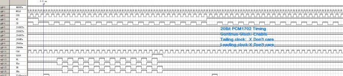
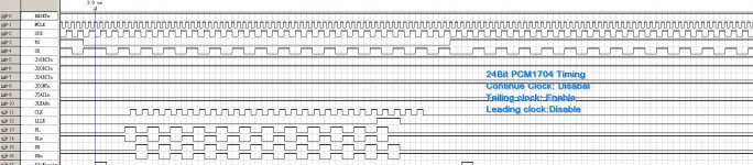
It took me quit a bit time revising the I2S to PCM daughter board design from SCK driven to MCLK driven. New design is 100% synchronized state machines. The performance get big improved. Now I can run 384KHz with 256Fs on the board. But I don't know which USB I2S could support.
1. 100% synchronized FPGA design with max inject MCLK going up to 127Mhz.
2. three word length jumpers, 16,18,20,24 bits output selectable
3. three option functions jumbers:
continue clk
tailing clk
leading clk
all jumbers are negative logic internally. Please note the new names.
4. I attached some simulation waveforms with different jumber setting.
all the simulations were run at 50Mhz MCLK for 128Fs. 100Mhz 256Fs got the almost the same result.
5. The tailing clk is reduced from 4 to 2 making PCM1704 benifit from it.
6. The leading clk new becomes optional.
Please let me know for any comment. FIFO board will be upgraded to support left justified format(which has nothing to do with this board).
Have a nice weekend.
I agree with you and Zsolt that as only the last n bits will be clocked in before latching. You clearly know more about all that high speed logic stuff and if you think that it has some advantages, leave it.
No problem. It was just me which did not get naming and status of the bits. As long as the combinations are safely described and not ambiguous (logic wise) it's OK.
This is a though one for me. I believe using 4 more clocks will be safe for both. As the DATA and LE lines are quiet anyway during conversion, I believe there is not much performance loss.
Very good. Will you use single flip flops (Potato?) for the sensitive clocks (LE and Bit clock?)
Actually, it helped me identify if all is OK (L/R difference)
Good, so the (dual) clock board is needed to select the correct clock freq and to provide the clean MCLK?
Will we still have the actual functionality on the dual clock board, i.e. the indication of fs and MCLK multiplicator?
Do you mean if you feed the FIFO with Sony format? Is that word length 24 bit, left justified, MSB first after word clock change, and Word Clock high = left channel?
Or do you mean that it should output Sony format, to feed eg. Andrea's SM5842?
All in all, great job Ian. thank you.
I would leave the "leading clock" for the reasons you mentioned, better to be on the safe side.
With 4 trailing clocks only PCM1702 would benefit of the stopped mode operation while for PCM1704 would be similar to continuous clock mode.
As PCM1704 is the newer and seems to be used by more diyers I would better support this - so to have 2 trailing clocks. But it's all one for me.
You would make fellow diyer andrea_mori happy
If you add another output format I have some arguments for the Left Justified over Sony Format:
- as I understood Andrea wants to connect the FIFO between a CD-Pro and his Sony Format input DAC board. As the CD-Pro outputs 16bit I2S you would have to add 16bit support to the converter to output a correct right justified format for him
- Left justified differs from I2S very slightly: latch should be negated and shifted with one clock - so needs less logic to implement
- digital filters from NPC, TI/BB, PMD all support Left Justified with multiple bit lengths, while Sony Format is supported only for 16bit data; except for NPCs
- the downside is that Andrea would have to make some minor pcb adjustments to set his board for Left Justified format - but hey, this is diy
All in all I'm fine with or without it.
Thanks, Zsolt
Hi Zsolit, Hi Vzs,
It took me quit a bit time revising the I2S to PCM daughter board design from SCK driven to MCLK driven. New design is 100% synchronized state machines. The performance get big improved. Now I can run 384KHz with 256Fs on the board. But I don't know which USB I2S could support.
1. 100% synchronized FPGA design with max inject MCLK going up to 127Mhz.
2. three word length jumpers, 16,18,20,24 bits output selectable
3. three option functions jumbers:
continue clk
tailing clk
leading clk
all jumbers are negative logic internally. Please note the new names.
4. I attached some simulation waveforms with different jumber setting.
all the simulations were run at 50Mhz MCLK for 128Fs. 100Mhz 256Fs got the almost the same result.
5. The tailing clk is reduced from 4 to 2 making PCM1704 benifit from it.
6. The leading clk new becomes optional.
Please let me know for any comment. FIFO board will be upgraded to support left justified format(which has nothing to do with this board).
Have a nice weekend.
Attachments
Last edited:
Hi Ian, very good. I'll look into these pictures, but not yet.
My nice will be here today and i have to help her solder a kit....a roboter kit. DIYRobot....
As for new functions of the fifo, are they reprogrammable in circuit?
The I2S to PCM daughter board is based on CPLD/FPGA, all this kind of designs are re-programble. Integrating it into FIFO board is possible, but I don't think it's a good idea because the output interface and connectors are different.
Enjoy your weekend.
Hi Ian,
Impressive progress. I reviewed your description (2 to 6) and the waveforms and everything looks good to me:
- I like that you added 16bit support
- The naming is clear like that (at least for me)
- Simulation waveforms looks good
- Leading clock selectable - too many goodies
How did you think it would work?
- I2S in and selectable I2S out or Left Justified Out
or
- selectable I2S in - I2S out or Left Justified in - Left Justified out
Thanks and enjoy your weekend (what is left),
Zsolt
Impressive progress. I reviewed your description (2 to 6) and the waveforms and everything looks good to me:
- I like that you added 16bit support
- The naming is clear like that (at least for me)
- Simulation waveforms looks good
- Leading clock selectable - too many goodies
Seems a logic decision not to put it on the converter daughter board.[...]FIFO board will be upgraded to support left justified format(which has nothing to do with this board)[...]
How did you think it would work?
- I2S in and selectable I2S out or Left Justified Out
or
- selectable I2S in - I2S out or Left Justified in - Left Justified out
Thanks and enjoy your weekend (what is left),
Zsolt
Hi Ian!
A little misunderstanding here....i was talking about this:
Oh, and for the different waveforms, they look good. I agree with about everything Zsolt has already stated. Nice there is 16bit also, who knows....
Anyway, hope you had a good weekend!
Ciao, Tino
The I2S to PCM daughter board is based on CPLD/FPGA, all this kind of designs are re-programble. Integrating it into FIFO board is possible, but I don't think it's a good idea because the output interface and connectors are different.
A little misunderstanding here....i was talking about this:
My question was if this can be updated easily on an existing FIFO board.[...]FIFO board will be upgraded to support left justified format(which has nothing to do with this board)[...]
Oh, and for the different waveforms, they look good. I agree with about everything Zsolt has already stated. Nice there is 16bit also, who knows....
Anyway, hope you had a good weekend!
Ciao, Tino
Hi Andrea,
In the above post, I'v already confirmed you can feed I2S signals directly from CDPro into FIFO.
Regards,
Does this mean that it also supports 32*fs?
(CDROM, VSLI Solution audio chips)
Does this mean that it also supports 32*fs?
(CDROM, VSLI Solution audio chips)
Yes, current version already support sck run at 32*Fs. But it standard I2S, not the right justified.
I remember you need a rigtht-justfied input tapping from a CDROM? 16bit of 24bit?
Hi Ian,
The vlsi audio chip (http://www.vlsi.fi/en/products/vs1053.html) are 32*fs I2S. The cdroms are 32*fs. Last I experimented with a TI ASRC, it required setting it as right justified. I'll have to get myself a logic analyzer to make sure.
But DACs support I2S, RJ, LJ so having these options, plus 32*fs, 48*fs and 64*fs clock will make it a "universal" device
Hi Ian,
The vlsi audio chip (VLSI Solution-VS1053 - Ogg Vorbis / MP3 / AAC / WMA / FLAC / MIDI Audio Decoder / Encoder Chip) are 32*fs I2S. The cdroms are 32*fs. Last I experimented with a TI ASRC, it required setting it as right justified. I'll have to get myself a logic analyzer to make sure.
But DACs support I2S, RJ, LJ so having these options, plus 32*fs, 48*fs and 64*fs clock will make it a "universal" device
Good point glt, but the right justified is kind of word length related, usually it's 16 and 24 bit. Is that works for you?
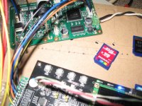
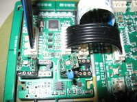
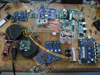
building up 'breadboard' for testing different options, clocks, references, regs IV etc for the dac that will drive my tweeters, the woofers are already covered with the NTD1 with another ackodac. some progress below, should power it all up tonight or tomorrow. I will try running Titan through the fifo as well as direct. it has its own clock fanout buffer and smaller fifo afaik and some rather nice clocks, so should be an interesting comparison, titan is capable of higher bandwidth than the fifo is in its current state, so i'll stick to 192 or below for the tests. the platform is normally mounted above the IV with the NTD1 thus the fairly useless set up here, though it will provide another layer of space for batteries, references etc for the rest of the testing
yes the 4 channel dac will be a 2 box affair with transformers and preregulators, battery charge circuit, along with some control circuitry in one case and the rest, DC onwards, dacs, input circuitry and output stages in the other.
its a pretty crazy build even for these 2 channels, first up i'm driving the wire BAL-BAL headphone amp directly and have altered the input circuit slightly to allow current mode coupling
please excuse the messy bench and rough and ready layout, i'll be switching things in and out so its only temporary and no thats not earwax on the cotton buds, its cardas rosin flux everything is currently floating in this build too, so thats another thing i'll be optimizing with this, the analogue stages including those in the dac should have a common ground reference, but the rest can float really as its either batteries, or a dedicated secondary winding for every consumer, so we'll see. the regs on the ackodac are all choke input so they float too
dacs arent what they used to be hey? ha
yes the 4 channel dac will be a 2 box affair with transformers and preregulators, battery charge circuit, along with some control circuitry in one case and the rest, DC onwards, dacs, input circuitry and output stages in the other.
its a pretty crazy build even for these 2 channels, first up i'm driving the wire BAL-BAL headphone amp directly and have altered the input circuit slightly to allow current mode coupling
please excuse the messy bench and rough and ready layout, i'll be switching things in and out so its only temporary and no thats not earwax on the cotton buds, its cardas rosin flux
everything is currently floating in this build too, so thats another thing i'll be optimizing with this, the analogue stages including those in the dac should have a common ground reference, but the rest can float really as its either batteries, or a dedicated secondary winding for every consumer, so we'll see. the regs on the ackodac are all choke input so they float toodacs arent what they used to be hey? ha
Attachments
Last edited:
- Home
- Source & Line
- Digital Line Level
- Asynchronous I2S FIFO project, an ultimate weapon to fight the jitter