Andrea, I don't think so. The schematic is strange anyway, Pin 5 and 10 should not be left open AFAIK.[...]
BTW do you think that I can feed 5842 using this schematics?
[...]
To feed SM5842, you'd need to delay WCK one bit clock (could be done before FIFO), then distribute the data to DIL and DIR, invert the WCK (it is exactly opposite polarized than I2S) or cheat, by feeding DIR with left data and vice versa. Also, in that case, you have to feed the left DAC with DOR and vice versa.
32 bit frames from I2S should not be a problem though.
Ian,
I would like to order FIFO kit, but I'm a bit confused.
As I said I want to feed FIFO kit directly from CD PRO I2S, then I would like to take I2S output and MCLK and feed digital filter NPC SM5842.
You tell me that SM5842 do not accept I2S format data, while Rregal in a previous post said that it can do it.
I found on the web the attached schematics that interface I2S with 5842, so I believe you're right.
BTW do you think that I can feed 5842 using this schematics?
If yes, do I need FIFO board only?
What frequency oscillator?
Anyone can help me?
Thanks in advance
Andrea
The schematic did show the DIR. Since all DIR support left justified format, I suspect that is. If me FIFO could support this format, you don't need anything else to feed signals into 5842.
Of course optionally selectable; seems it will support many.So you mean to have it as an optionally selectable format, as would be the stopped clock operation?
Then it's OK of course")
Andrea, I don't think so. The schematic is strange anyway, Pin 5 and 10 should not be left open AFAIK.
To feed SM5842, you'd need to delay WCK one bit clock (could be done before FIFO), then distribute the data to DIL and DIR, invert the WCK (it is exactly opposite polarized than I2S) or cheat, by feeding DIR with left data and vice versa. Also, in that case, you have to feed the left DAC with DOR and vice versa.
32 bit frames from I2S should not be a problem though.
Zinsula,
it seems that 5842 is feeded like Sony data format.
But quad flip-flop HC175 do not act what you say?
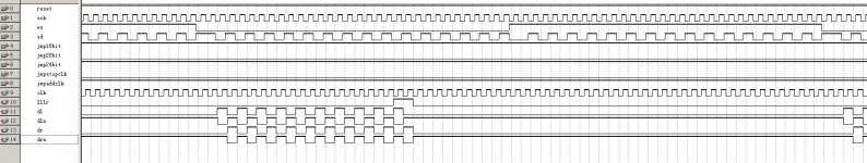
I2S to PCM convertor real verilogHDL simulation
Hi zinsula, Hi vzs,
I attached simulation result waveforms generated by real synthesizable verilogHDL source code. Please note the five jumpers. Three of them for selecting data length; one of them to decide if going with stopping clock function; If stoping clock function is enabled, the another one selecting if delay the latching signal (for ASD18XX and PCM63) or add four more clocks without delay the latching signal (for PCM1702/4).
Me too got a bit confusing on the PCM1702/04 timing, please confirm the added clock number is 4 (now is 4) or 2.
And another thing is how do you think about the finial flip-flop re-clock function?
Without it the finial phase noise on the latching signal will be 12 dB more than the original mclk (because sck is a generated clk which is already 6dB more phase noise than the original mclk). (each signal generated by a clock will roughly 6dB more phase noise than that clock).
* Please find the file names of each attached pictures for what they are.
Small project with a lot of details.
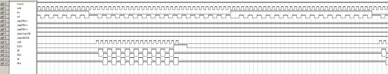
Hi zinsula, Hi vzs,
I attached simulation result waveforms generated by real synthesizable verilogHDL source code. Please note the five jumpers. Three of them for selecting data length; one of them to decide if going with stopping clock function; If stoping clock function is enabled, the another one selecting if delay the latching signal (for ASD18XX and PCM63) or add four more clocks without delay the latching signal (for PCM1702/4).
Me too got a bit confusing on the PCM1702/04 timing, please confirm the added clock number is 4 (now is 4) or 2.
And another thing is how do you think about the finial flip-flop re-clock function?
Without it the finial phase noise on the latching signal will be 12 dB more than the original mclk (because sck is a generated clk which is already 6dB more phase noise than the original mclk). (each signal generated by a clock will roughly 6dB more phase noise than that clock).
* Please find the file names of each attached pictures for what they are.
Small project with a lot of details
.Attachments
Last edited:
Hi Ian,[...]Me too got a bit confusing on the PCM1702/04 timing, please confirm the added clock number is 4 (now is 4) or 2.[...]
PCM1704 needs 2 clocks, PCM1702 needs 4 clocks, see the attached descriptions from those datasheets.
If there is to choose which one, i'd say PCM1704, as I have the impression that more people uses them. But I really do not want to press decision on this one, I do not have neither of those DAC's.
Attachments
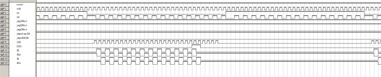
OK i checked the three examples. Some remarks[...]I attached simulation result waveforms generated by real synthesizable verilogHDL source code. Please note the five jumpers. Three of them for selecting data length; one of them to decide if going with stopping clock function; If stoping clock function is enabled, the another one selecting if delay the latching signal (for ASD18XX and PCM63) or add four more clocks without delay the latching signal (for PCM1702/4).[...]
ContinueClk20bit:
Data seems OK
LE OK
Bit clock stop OK
Do I get it right, that if i see the jumper line, the jumper is OFF?
So, in this case,
jmp18bit=0, jmp20bit=1, jmp24bit=0, jmpstopclk=1 (why? it is not stopped); jmpaddclk=0
StopClkDelayLatch18bit:
Data seems OK
LE OK
Bit clock stop OK
BUT: i count 19 bits, not 18, therefore the MSB left data is 0, should be 1.
jmp18bit=1, jmp20bit=0, jmp24bit=0, jmpstopclk=0 (why? it is stopped); jmpaddclk=0
StopClkWith4More24bit:
Data seems OK
LE OK
Added clocks after LE going negative is OK (see my other post whether 2 or 4 clocks)
Bit clock stop OK
BUT: i count 25 bits, not 24, therefore the MSB left data is 0, should be 1.
jmp18bit=1 (?), jmp20bit=1 (?), jmp24bit=0 (?), jmpstopclk=0 (why? it is stopped); jmpaddclk=1
Ian, all in all that looks very good!
Thank you, Tino
[...]And another thing is how do you think about the finial flip-flop re-clock function?
Without it the finial phase noise on the latching signal will be 12 dB more than the original mclk (because sck is a generated clk which is already 6dB more phase noise than the original mclk). (each signal generated by a clock will roughly 6dB more phase noise than that clock).[...]
I think, CLK and LLLR in your diagrams should be reclocked, as you did it on your clock board with separate flip-flops (pico gates?).
So we could "inject" the master clock from your clock board with the U.FL cable, isn't it?
Data is not that important, if you need it to reclock for timing/realignment purposes, the four data lines could be reclocked with a quad or whatever flip flop.
Thank you!
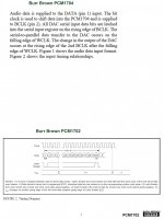
I believe the pin description table in SM5842 manual is screwed up a bit: see page 3, explanation of pins 5,10 - there is no such pin like IW2N/DIL or IW1N/DIR and in the explanation of pin10 it would be logical to mention INF1N not INF2N.it seems that 5842 is feeded like Sony data format.
But quad flip-flop HC175 do not act what you say?
Indeed, your schematic from #375 is configured for Sony format: INF1N (pin4) is LOW
But if this format is selected the bit length should be selected as well: see description pin5, 10 - but in the schematics these pins were left open-this is not correct
I think zinsula suggested to modify the input format from Sony-format to left justified-LR data alternating and he suggested a simple way to change I2S format to left justified format. For this format you would have to make INF1N HIGH and DI/INF2N LOW (your data input being now IW1N/DIL and IW2N/DIR)
If Ian will manage to squeeze the Left-Justified format into its converter you will not need the I2S-to-left justified logic suggested by zinsula.
The 75VHC175 flip-flops simply reclocks the data comming out from SM5842 with the master clock.
Well then it's OK and you do not have to alter the data.[...]it seems that 5842 is feeded like Sony data format.[...]
But I thougt your transport is putting out I2S? Sony format is not I2S!
No, it is just there for reclocking.[...]But quad flip-flop HC175 do not act what you say?
What i said is that if you have true I2S, you have to modify the data before SM5842.
In your schematic, i see nothing in front of SM5842.
74VHC175 is between SM5842 and DAC's (are these PCM63?)
Hi Ian,[...]I attached simulation result waveforms generated by real synthesizable verilogHDL source code[...]
It looks promising. I also have some remarks:
Five jumper selectors
- it seems that beside jmpstopclk you used negative logic to set their function
- according to the simulations they look correct, but this negative/positive logic mixing is a bit confusing. Would be nice to be consistent and use either negative or positive logic for all
Data and clock lines for all three images
- is confusing that the MSB of the right channel starts with 0 while the MSB of the left channel with 1; so it looks like they are delayed by one clock, but probably not
- for stopped clock mode I also count +1 clock but I don't think this is an issue since only the last X bits will be transferred to the parallel DAC registers (after latch has gone low)
Concerning reclocking I share zinsula's opinion from #388.
A suggestion about board layout: it would be nice to be stack-able above the clock board - probably same size. If it's input would come from the FIFO board then the input connector could be in same position as on the clock board.
Thanks, Zsolt
vzs zinsula,
thanks
.. so I have to wait Ian to modify FPGA logic ... the best way I understand
Ian
I'm in your hands..
Andrea
Hi Andrea, Don't worry about that, I'm the guy.
... funny
I need more than a little help, I like this project but I like also my SM5842 and PCM63. They are waiting for the right implementation.
Any help would appreciate
Andrea
OK i checked the three examples. Some remarks
ContinueClk20bit:
Data seems OK
LE OK
Bit clock stop OK
Do I get it right, that if i see the jumper line, the jumper is OFF?
So, in this case,
jmp18bit=0, jmp20bit=1, jmp24bit=0, jmpstopclk=1 (why? it is not stopped); jmpaddclk=0
StopClkDelayLatch18bit:
Data seems OK
LE OK
Bit clock stop OK
BUT: i count 19 bits, not 18, therefore the MSB left data is 0, should be 1.
jmp18bit=1, jmp20bit=0, jmp24bit=0, jmpstopclk=0 (why? it is stopped); jmpaddclk=0
StopClkWith4More24bit:
Data seems OK
LE OK
Added clocks after LE going negative is OK (see my other post whether 2 or 4 clocks)
Bit clock stop OK
BUT: i count 25 bits, not 24, therefore the MSB left data is 0, should be 1.
jmp18bit=1 (?), jmp20bit=1 (?), jmp24bit=0 (?), jmpstopclk=0 (why? it is stopped); jmpaddclk=1
Ian, all in all that looks very good!
Thank you, Tino
I think, CLK and LLLR in your diagrams should be reclocked, as you did it on your clock board with separate flip-flops (pico gates?).
So we could "inject" the master clock from your clock board with the U.FL cable, isn't it?
Data is not that important, if you need it to reclock for timing/realignment purposes, the four data lines could be reclocked with a quad or whatever flip flop.
Thank you!
Hi Ian,
It looks promising. I also have some remarks:
Five jumper selectors
- it seems that beside jmpstopclk you used negative logic to set their function
- according to the simulations they look correct, but this negative/positive logic mixing is a bit confusing. Would be nice to be consistent and use either negative or positive logic for all
Data and clock lines for all three images
- is confusing that the MSB of the right channel starts with 0 while the MSB of the left channel with 1; so it looks like they are delayed by one clock, but probably not
- for stopped clock mode I also count +1 clock but I don't think this is an issue since only the last X bits will be transferred to the parallel DAC registers (after latch has gone low)
Concerning reclocking I share zinsula's opinion from #388.
A suggestion about board layout: it would be nice to be stack-able above the clock board - probably same size. If it's input would come from the FIFO board then the input connector could be in same position as on the clock board.
Thanks, Zsolt
Hi guys, you made very good points
1, The one more clk, I call it "leading clock", is just for warm up the shift registers, avoid any potential glitch when switching from the stopping mode to the working mode. Logic wise, we don't need that additional clock. Any way, only last Nbit before the falling edge of latching signal will be latched into DAC, anything else will be shift away. Please let me know your point, leave it or remove it?
2, Each the jumper has a internal programble pull-up resister. So, the default logic is '1' if not be shorted to GND. I will leave the most possible default setting as 'open' to reduce the chance of 'jumping'. I'll have a very clear true table in the PDF file. Maybe, I need rename some of them to make the logic more clear.
3, PCM1702/04 need 2 and 4 clks, does that mean 4 more clks is safe for both of them?
4, As you all agree re-clock by the original mclk is a better solution than the second-generation sck, I'll inject the mclk from the clock board to make all FPGA logic synchronized with the original clock. In this case, the estimated Fmax could go up to 120MHz, finial performance will gain from this configuration.
5, On the simulation waveform, the 32bit I2S left channel data is 0xAAAAAAAA, while the right is 0x55555555, please just make sure the finial PCM Nbit data are correct correspondingly(MSB to MSB).
6, For sure, this small convertor board will be stacked over the clock board of the FIFO KIT with the same size and screw positions. I2S signals will be input directly form FIFO rather than from clock board to make the clock quieter
. (we don't need the re-clocked I2S input, re-clocking will be made at finial stage)7, Do you think this little convertor board need support an optional 'SONY' format beside the default I2S format?
Cheers,
And another thing is how do you think about the finial flip-flop re-clock function?
Without it the finial phase noise on the latching signal will be 12 dB more than the original mclk (because sck is a generated clk which is already 6dB more phase noise than the original mclk). (each signal generated by a clock will roughly 6dB more phase noise than that clock).
I'm not sure how you arrive at the +6dB phase noise from the logic. I would like to know.
In the testing I have done recently I'm seeing more issues around deterministic noise that random phase noise. I would use reclocking D latches, possibly the Potato stuff and run them on an isolated supply. It only takes a little supply noise to modulate a clock in a gate, especially when we are looking at -120 to -150 dB.
I agree with you and Zsolt that as only the last n bits will be clocked in before latching. You clearly know more about all that high speed logic stuff and if you think that it has some advantages, leave it.[...]
1, The one more clk, I call it "leading clock", is just for warm up the shift registers, avoid any potential glitch when switching from the stopping mode to the working mode. Logic wise, we don't need that additional clock. Any way, only last Nbit before the falling edge of latching signal will be latched into DAC, anything else will be shift away. Please let me know your point, leave it or remove it?[...]
No problem. It was just me which did not get naming and status of the bits. As long as the combinations are safely described and not ambiguous (logic wise) it's OK.[...]
2, Each the jumper has a internal programble pull-up resister. So, the default logic is '1' if not be shorted to GND. I will leave the most possible default setting as 'open' to reduce the chance of 'jumping'. I'll have a very clear true table in the PDF file. Maybe, I need rename some of them to make the logic more clear.[...]
This is a though one for me. I believe using 4 more clocks will be safe for both. As the DATA and LE lines are quiet anyway during conversion, I believe there is not much performance loss.[...]
3, PCM1702/04 need 2 and 4 clks, does that mean 4 more clks is safe for both of them?
[...]
Very good. Will you use single flip flops (Potato?) for the sensitive clocks (LE and Bit clock?)[...]
4, As you all agree re-clock by the original mclk is a better solution than the second-generation sck, I'll inject the mclk from the clock board to make all FPGA logic synchronized with the original clock. In this case, the estimated Fmax could go up to 120MHz, finial performance will gain from this configuration.[...]
Actually, it helped me identify if all is OK (L/R difference)[...]
5, On the simulation waveform, the 32bit I2S left channel data is 0xAAAAAAAA, while the right is 0x55555555, please just make sure the finial PCM Nbit data are correct correspondingly(MSB to MSB).[...]
Good, so the (dual) clock board is needed to select the correct clock freq and to provide the clean MCLK?[...]
6, For sure, this small convertor board will be stacked over the clock board of the FIFO KIT with the same size and screw positions. I2S signals will be input directly form FIFO rather than from clock board to make the clock quieter
Will we still have the actual functionality on the dual clock board, i.e. the indication of fs and MCLK multiplicator?
Do you mean if you feed the FIFO with Sony format? Is that word length 24 bit, left justified, MSB first after word clock change, and Word Clock high = left channel?[...]
7, Do you think this little convertor board need support an optional 'SONY' format beside the default I2S format?
[...]
Or do you mean that it should output Sony format, to feed eg. Andrea's SM5842?
All in all, great job Ian. thank you.
Last edited:
Yes, using separate D-Flip-Flops (i mean using only one Flip Flop per case) for the important signals will allow to decouple their supplies, minimizing the crostalk on the supply line. Inductor will help to isolate them from each other.[...]I would use reclocking D latches, possibly the Potato stuff and run them on an isolated supply. It only takes a little supply noise to modulate a clock in a gate, especially when we are looking at -120 to -150 dB.
As i understood the Potato stuff, it is about them using balanced signals, which would result in less power supply modulation. As in our beloved balanced amps or preamps....
Last edited:
I would leave the "leading clock" for the reasons you mentioned, better to be on the safe side.1, The one more clk, I call it "leading clock", is just for warm up the shift registers, avoid any potential glitch when switching from the stopping mode to the working mode. Logic wise, we don't need that additional clock. Any way, only last Nbit before the falling edge of latching signal will be latched into DAC, anything else will be shift away. Please let me know your point, leave it or remove it?
With 4 trailing clocks only PCM1702 would benefit of the stopped mode operation while for PCM1704 would be similar to continuous clock mode.3, PCM1702/04 need 2 and 4 clks, does that mean 4 more clks is safe for both of them?
As PCM1704 is the newer and seems to be used by more diyers I would better support this - so to have 2 trailing clocks. But it's all one for me.
You would make fellow diyer andrea_mori happy7, Do you think this little convertor board need support an optional 'SONY' format beside the default I2S format?
If you add another output format I have some arguments for the Left Justified over Sony Format:
- as I understood Andrea wants to connect the FIFO between a CD-Pro and his Sony Format input DAC board. As the CD-Pro outputs 16bit I2S you would have to add 16bit support to the converter to output a correct right justified format for him
- Left justified differs from I2S very slightly: latch should be negated and shifted with one clock - so needs less logic to implement
- digital filters from NPC, TI/BB, PMD all support Left Justified with multiple bit lengths, while Sony Format is supported only for 16bit data; except for NPCs
- the downside is that Andrea would have to make some minor pcb adjustments to set his board for Left Justified format - but hey, this is diy
All in all I'm fine with or without it.
Thanks, Zsolt
Last edited:
- Home
- Source & Line
- Digital Line Level
- Asynchronous I2S FIFO project, an ultimate weapon to fight the jitter