Here is a 3.3V regulator I'm using. I'm still verifying its performance. The sim shows .7 nV/ rtHz which is really really low. I have checked it with my normal stuff and its too low noise for a real reading so I'm building a tester for it, not easy. I had to transformer couple the input to get a low enough noise input.
It does work and seems to improve the sound from the digital side.
It does work and seems to improve the sound from the digital side.
An externally hosted image should be here but it was not working when we last tested it.
Here is a 3.3V regulator I'm using. The sim shows .7 nV/ rtHz which is really really low.
Interesting topologies and impressed sim result.
Yes, you are right, low noise power supply is very very important for jitter sensitive applications. But it's very difficult to measure after reach a certain level
") .
. What sim software do you use? Did you take the inductance of capacitors and the PCB into account in your sim? How about the source and load transient response? 431 itself is not a super low noise reference, did you try any thing better? Ian
Ian:
Here are some links that you may enjoy, about a similar memory buffer effort.
They are all in Japanese, but include enough schematics and graphs that you shouldn't be bored.
http://easyaudiokit.hobby-web.net/bekkan/memory/memorybuffermanual.pdf
http://easyaudiokit.hobby-web.net/bekkan/memory/memorybuffer.html
http://easyaudiokit.hobby-web.net/bekkan/memory/memory2.html
http://easyaudiokit.hobby-web.net/bekkan/memory/memory3.html
http://easyaudiokit.hobby-web.net/bekkan/memory/bugfix.html
http://easyaudiokit.hobby-web.net/bekkan/manual/adaptermanual.pdf
http://easyaudiokit.hobby-web.net/bekkan/memory/memory3.html
http://easyaudiokit.hobby-web.net/bekkan/MBacc/MBacc.html
http://easyaudiokit.hobby-web.net/bekkan/manual/SPDIF_Freq_checker.pdf
http://easyaudiokit.hobby-web.net/bekkan/manual/SPDIF_Freq_CheckerV2_PIC_VERSION_.pdf
kind regards, jonathan carr
Interesting topologies and impressed sim result.
Yes, you are right, low noise power supply is very very important for jitter sensitive applications. But it's very difficult to measure after reach a certain level
What sim software do you use? Did you take the inductance of capacitors and the PCB into account in your sim? How about the source and load transient response? 431 itself is not a super low noise reference, did you try any thing better? Ian
The sim was with Ltspice. The parasitic L's and C's won't change the noise since they are noiseless. The circuit is a little non-intuitive. The actual regulator is the Sziklai pair. The reference voltage is at the junction of R11 and C7. R11 is large and C7's reactance is small so the effective noise resistance is very low. Q1's junction dominates the noise sources and it is not in saturation so its amplifying. The current passes through Q2 in common base configuration which is lower noise than a follower would be.
The 431 stabilizes the voltage but its isolated by the 1K 500 uF combo so its noise doesn't get into the circuit. Its response is slow and its only used to steer the DC value. A crystal oscillator working properly is about as dynamic a load as a resistor so transient response of the circuit isn't important in that application. This circuit should be pretty good for a class a low level preamp circuit as well, again no supply dynamics. Logic is another story however. Most logic has really high dynamics and its best dealt with by local bypassing with enough storage for its demands.
This circuit is also pretty cheap to implement. The cost of low noise LDO's gets quite high ($5.00 + for the ones I was looking at) and needing multiples got a little crazy.
Ian:
Here are some links that you may enjoy, about a similar memory buffer effort.
They are all in Japanese, but include enough schematics and graphs that you shouldn't be bored.
kind regards, jonathan carr
Thank you so much for sharing your projcet with us, Jcarr. Great job! Did you design it by yourself? Very classical schematics, as well as the PCB. I couldn't imagine how difficult it would be to achieve a whole I2S buffer by logic ICs only.
I hope I understood Japanese
. But at least I could learn something from the schematics and the pictures. How many kinds of oscillators did you try? Did you find something really nice? It seems the projcet was finished couples of years ago, so I suspect you get some new ideas now.Have a nice weekend. Ian
I don't think that's Jonathan's work. He specializes in exceptional phono cartridges and preamps. If it were all point to point wire with no pcb anywhere and looked like macrame I would believe it. It "might" sound better. It would also be a real work of art and impossible to build.
The sim was with Ltspice. The parasitic L's and C's won't change the noise since they are noiseless. The circuit is a little non-intuitive. The actual regulator is the Sziklai pair. The reference voltage is at the junction of R11 and C7. R11 is large and C7's reactance is small so the effective noise resistance is very low. Q1's junction dominates the noise sources and it is not in saturation so its amplifying. The current passes through Q2 in common base configuration which is lower noise than a follower would be.
This circuit is also pretty cheap to implement. The cost of low noise LDO's gets quite high ($5.00 + for the ones I was looking at) and needing multiples got a little crazy.
Hi Demian,
Thank you so much for those answers. Make sence. It's very smart design and I think I need take time to analyze it.
How much current it could deliver? What is the most optimized current range? Is it possible being extended to power 300mA load? I'm looking for something to replace my batteries
. But I still don't have time going any deep into this issue. Nice weekend. Ian
The design with the 2N4403 pass transistor will handle 150 mA if the raw supply is 5v or less. A heatsink is not required but a good idea. A larger transistor could be used to handle more current. That will need some analysis but should not be too difficult. I may build a 15V version for some oven oscillators I have that draw 750 mA on startup. That will definitely need some more sophistication. I have some ideas using an LM317 to deal with heat and short circuit issues.
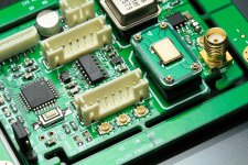
My second clock board: Double XO Clock MK2
I just finished assembling and testing my double XO clock board MK2 last weekend. I have to say, comparing with previous one, the new clock board is better. The new design has the following highlighted features:
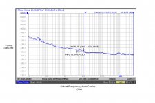
1. Equipped with dedicated clock fan-out buffers switching between the two oscillators and distributing clock signals point to point. The fan-out buffer comes with only 29fs additive jitter which is unbelievable. I attached the phase noise plot of this buffer just for reference.
2. Powering two oscillators at same time with 9uV RMS low noise high PSRR LDO and independent EMI suppression filters.
3. Re-clocking the I2S signals with 600MHz Potato low noise GHz PO74G74, which is the fastest flip-flop with LVCMOS/LVTTL output I could find out so far. Although OS and DS DACs are not that sensitive to the jitter from I2S signals because their internal logic are synchronized with MCLK, but NOS DACs are! It seems that my TDA1541 NOS DAC will benefit a lot from this low jitter I2S re-clock circuit.
4. Switching the clock instantly once the Fs being changed.
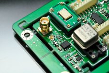
5. Introducing 6GHz U.FL RF connectors and cables into the new clock board for MCLK and I2S output signals.
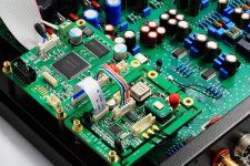
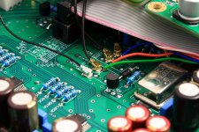
I really love those U.FL connectors and cables! They are compact, reliable, soft and very easy to assemble. Now I could get rid of the big SMA connectors as well as its inflexible cables (however, I left an optional SMA position which could be suitable for both SMA and U.FL connector just in case I need it sometime). Actually, the U.FL and IPX is almost the same thing and they are 100% compatible from each other. They have different name just because of the patent. Both of them show very good performance during my test. The U.FL cables could be easily sourced from Digikey, while the customized length cables can be ordered directly from the IPX manufacturer’s website.
Another advantage is that the U.FL connector is a kind of very small SMT component; it’s very easy being soldered directly to the signal pad and the GND plate underneath on a DAC PCB without any flying wires. And furthermore, with those 50 ohm RF cables and source impedance matching, the quality of the I2S signals get much improved.
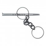
I didn’t select the W.FL connectors and cables, because they are too small and a bit harder to assemble. Special tool is needed to pull out the U.FL cable from the connector. Otherwise, both of the cable socket and the fingernail might be broken. That tool is available from digikey, but DIY a one is not a difficult job.
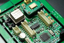
I attached the pictures of the new hookup between the FIFO, double XO MK2 clock board and the WM8741 DAC. It looks better because of those U.FL connectors and cables.
Now, I'm using the balanced output of the WM8741 DAC and replacing the Op Amps with OPA1612. It sounds better. I collected quite a few clock oscillators so far from different sources, but my dream clock is still keeping absence.
Thanks 1audio, simmconn, qusp, Nazar_lv and many other friends from this audiophile community. Thank you so much for those comments, suggestions and recommendations.
Other features keep no change, they are:
1. Frequency supported
.44.1KHz 16bit (24bit/32bit ready)
.48KHz 16bit (24bit/32bit ready)
.88.2KHz 16bit/24bit (32bit ready)
.96KHz 16bit/24bit (32bit ready)
.176.4KHz 16bit/24bit/32bit
.192KHz 16bit/24bit/32bit
2. Switching the MCLK and *Fs automatically according to the input I2S stream;
3. Open concept for XO selection
XO options for the socket U1:
11.2896MHz (go 44.1K and 88.2K)
Or, 22.5792MHz (go 44.1K, 88.2K and 176.4K)
14Pin or 9Pin standard XO with 3.3V Vcc
XO options for the socket U2:
12.2880MHz (go 48K and 96K)
Or, 24.5760MHz (go 48K, 96K and 192K)
14Pin or 9Pin standard XO with 3.3V Vcc
4. Manual frequency switching button for optional standalone working mode;
5. Frequency settings will be saved and applied automatically at next power up.
I just finished assembling and testing my double XO clock board MK2 last weekend. I have to say, comparing with previous one, the new clock board is better. The new design has the following highlighted features:
1. Equipped with dedicated clock fan-out buffers switching between the two oscillators and distributing clock signals point to point. The fan-out buffer comes with only 29fs additive jitter which is unbelievable. I attached the phase noise plot of this buffer just for reference.
2. Powering two oscillators at same time with 9uV RMS low noise high PSRR LDO and independent EMI suppression filters.
3. Re-clocking the I2S signals with 600MHz Potato low noise GHz PO74G74, which is the fastest flip-flop with LVCMOS/LVTTL output I could find out so far. Although OS and DS DACs are not that sensitive to the jitter from I2S signals because their internal logic are synchronized with MCLK, but NOS DACs are! It seems that my TDA1541 NOS DAC will benefit a lot from this low jitter I2S re-clock circuit.
4. Switching the clock instantly once the Fs being changed.
5. Introducing 6GHz U.FL RF connectors and cables into the new clock board for MCLK and I2S output signals.
I really love those U.FL connectors and cables! They are compact, reliable, soft and very easy to assemble. Now I could get rid of the big SMA connectors as well as its inflexible cables (however, I left an optional SMA position which could be suitable for both SMA and U.FL connector just in case I need it sometime). Actually, the U.FL and IPX is almost the same thing and they are 100% compatible from each other. They have different name just because of the patent. Both of them show very good performance during my test. The U.FL cables could be easily sourced from Digikey, while the customized length cables can be ordered directly from the IPX manufacturer’s website.
Another advantage is that the U.FL connector is a kind of very small SMT component; it’s very easy being soldered directly to the signal pad and the GND plate underneath on a DAC PCB without any flying wires. And furthermore, with those 50 ohm RF cables and source impedance matching, the quality of the I2S signals get much improved.
I didn’t select the W.FL connectors and cables, because they are too small and a bit harder to assemble. Special tool is needed to pull out the U.FL cable from the connector. Otherwise, both of the cable socket and the fingernail might be broken. That tool is available from digikey, but DIY a one is not a difficult job.
I attached the pictures of the new hookup between the FIFO, double XO MK2 clock board and the WM8741 DAC. It looks better because of those U.FL connectors and cables.
Now, I'm using the balanced output of the WM8741 DAC and replacing the Op Amps with OPA1612. It sounds better. I collected quite a few clock oscillators so far from different sources, but my dream clock is still keeping absence.
Thanks 1audio, simmconn, qusp, Nazar_lv and many other friends from this audiophile community. Thank you so much for those comments, suggestions and recommendations.
Other features keep no change, they are:
1. Frequency supported
.44.1KHz 16bit (24bit/32bit ready)
.48KHz 16bit (24bit/32bit ready)
.88.2KHz 16bit/24bit (32bit ready)
.96KHz 16bit/24bit (32bit ready)
.176.4KHz 16bit/24bit/32bit
.192KHz 16bit/24bit/32bit
2. Switching the MCLK and *Fs automatically according to the input I2S stream;
3. Open concept for XO selection
XO options for the socket U1:
11.2896MHz (go 44.1K and 88.2K)
Or, 22.5792MHz (go 44.1K, 88.2K and 176.4K)
14Pin or 9Pin standard XO with 3.3V Vcc
XO options for the socket U2:
12.2880MHz (go 48K and 96K)
Or, 24.5760MHz (go 48K, 96K and 192K)
14Pin or 9Pin standard XO with 3.3V Vcc
4. Manual frequency switching button for optional standalone working mode;
5. Frequency settings will be saved and applied automatically at next power up.
Attachments
-
 FanoutBufferPhaseNoisePlot.JPG117.5 KB · Views: 2,451
 -
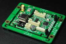 DoubleXOClockMK2.JPG587.6 KB · Views: 2,496
 -
 DoubleMCLKoutputAndFanoutBuffer.JPG414.6 KB · Views: 2,360
 -
 GHzI2sReClocking.JPG591.5 KB · Views: 2,283
 -
 U.FLconnectors.JPG578.8 KB · Views: 1,017
 -
 FIFOtoWM8741HookupWithU.FL.JPG631.5 KB · Views: 947
 -
 ModdingDACwithU.FL.JPG477.9 KB · Views: 938
 -
 U.FL-LP(V)-N-2.jpg70.7 KB · Views: 963
Last edited:
Hi, Ian
How do I say ?....Ummm
I just found some error on our WM8741 designed.
1. Our WM8741 is not differential mode summing
2. LPF is not good enough for HI-END
\Now I'm on the hard work of ESS9018 parallel 8DACs per channel and when it completed I shall send you asap
Thanks
Anadigit
How do I say ?....Ummm
I just found some error on our WM8741 designed.
1. Our WM8741 is not differential mode summing
2. LPF is not good enough for HI-END
\Now I'm on the hard work of ESS9018 parallel 8DACs per channel and when it completed I shall send you asap
Thanks
Anadigit
Hi Ian,
Very nicely done board!
I was a bit skeptical about the o-ring suspension design for the clock board, until I saw something similar in an HP 8662A signal generator, which has been used as a low phase-noise reference for many years. I was working on a fix-upper for the past two weeks. Very solid machine. My unit is apparently aged and has multiple problems. But it is fun to work on and eventually bring it back to life (and to spec later).
BR,
simmconn
How nice to have such a plot! How did you obtain this ? Did you measure it by yourself? Which instrument did they use?1. ... I attached the phase noise plot of this buffer just for reference.
How nice to have such a plot! How did you obtain this ? Did you measure it by yourself? Which instrument did they use?
Hi Bunpei,
I hope I had that oscillator, if so, that would be one of my dream oscs
.This phase noise plot was originally from the manufacturer of the clock fanout buffer . There are two curves, one of them is for the input clock and the other one is for the output clock from the fanout buffer . The second one is very close to the first, that indicates the additive jitter of the fanout buffer is very small (29fs). Usually they use equipments like Agilent E5052A making this kind of measurement. Ian
Ian,
You are an artist.
Regards,
George
Thanks George,
Technologies is a kind of art, especially for our audiophiles
.Best Regards,
Ian
Why would a shunt regulator sound better running a crystal oscillator? The key issue with an XO is low noise. Number two would be high isolation from the primary supply to prevent modulation from external sources like the audio/data stream. A good XO will have zero dynamics as a load. I supplied a regulator above with 20 dB lower noise than any I have seen published. It could be folded into a shunt regulator but that may make no difference except for requiring some really sophisticated current source to get to the same place.
Ian:
What are you using for the clock buffer?
Making a measurement of the phase noise is not trivial but is not too hard to do with pretty available stuff. For a buffer you only need one oscillator, a suitable rf mixer and a good fft. Its tedious to setup and calibrate. For an audio system its easier to look at the spurious outputs on the audio outputs, less hardware is needed and it will show the effects of everything in the chain.
Hi Ian,
Very nicely done board!
I was a bit skeptical about the o-ring suspension design for the clock board, until I saw something similar in an HP 8662A signal generator, which has been used as a low phase-noise reference for many years.BR,
simmconn
Thanks simmconn,
Did you fix up your super oscillator? Please just let me know what it sounds like
.At least two things are sensitive to the mechanical vibration. One is the crystal inside the XO and the other is the MLCC due to its piezoelectric effect. So, theoretically the rubber ring works for isolating that vibration. But, by how much, I didn't confirm.
Regards,
Ian
- Home
- Source & Line
- Digital Line Level
- Asynchronous I2S FIFO project, an ultimate weapon to fight the jitter