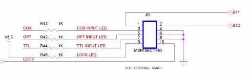
Ian, thanks for your reply. I did some measurement on the 10 pins and found the following :
Niether Pin 1 nor 2 is connected to GND, and I can't measure any voltage on both pins, should I need a relay to short these pins for input selection?
Pins 3, 5, 7 are GND, and 2, 4, 6 can provide logical high for input detection.
Pin 9 and 10 are not connected to GND or 5V, so I need additional circuit to provide logic "high" for SPDIF lock indication.
Are my measurement and assumption correct?
Hi bigpandahk
You did correct measurement.
1, The key button is scaned by the internal state machine, so the logic level is not fixed or determined, using a relay is a good idea. The 'on' pluse could be around 100ms;
2, Defferent from other LEDs, the lock LED is an active low logic;
I attached the schmatic of the panel interface below, everything should be clear.
Have a nice weekend.
Ian
Attachments
well just completed reading this whole thread .
one oher member asked the same question without answer:
Can the fifo feed i2s to 2 buf3 for dual mono and if so how?
Hi necplusultra,
I don't think there is any problem to interface FIFO with BIII at mono mode. If you know how to setup BIII running mono mode with branching all signals into two BIII baords, then everything will be very easy.
The only thing is, if you want to run the sync clock mode, you have to remove local XOs and feed the MCLK into the two BIII board with two U.FL cables.
Have a nice weekend.
Ian
there is no difference in the signal sent to each dac with dual mono, both are sent the same stereo signal as if you were feeding just one. the difference is on the dac board. for dual mono or the other dual modes each dac/device is assigned a number 0 or 1 (dev0 or dev1) on start up; depending on which address each dac takes, it uses only the information in the stereo i2s stream that is pertinent to its channel. so dev0 will use only right channel information and dev1 will use only left.
no splitting needed, just use the 2 outputs on the clock board to send the same i2s to both
no splitting needed, just use the 2 outputs on the clock board to send the same i2s to both
thanks QUSP and Ian,
I was not sure how to connect the i2s to 2 Bufs. So basically, I would require an extra BIII adapter kit to send the the 2nd 12s from clock board. I presume the synch/asynch config would be the same as for stereo buf3.
One more question, how do you guys remove the xo from the buf board?
I was not sure how to connect the i2s to 2 Bufs. So basically, I would require an extra BIII adapter kit to send the the 2nd 12s from clock board. I presume the synch/asynch config would be the same as for stereo buf3.
One more question, how do you guys remove the xo from the buf board?
Hi Ian
I am writing the Arduino program to select the input of your S/PDIF and indicate on the LCD, there is no LED for the backdoor I2S on the connector for external control panel interface. Any other way for me to get the signal?
Hi bigpandahk,
I would be very much interested in your project, as I will have the same need. I am using Arduino board as well with glt's code. Works awesome. Here is the link for my ever changing project.
Hifiduino with VFD Display H i F i D U I N O
Hi bigpandahk,
I would be very much interested in your project, as I will have the same need. I am using Arduino board as well with glt's code. Works awesome. Here is the link for my ever changing project.
Hifiduino with VFD Display H i F i D U I N O
Hi AR2
Your projects are beautiful, where did you buy all those nice connectors (USB, coaxial) and the case? Are you panels done by Front panel express?
That's a good idea. But the low phase noise doubler would be the key part. Any reference design?
Ian
Here is a first pass. The principle is to generate a positive edge on each transition. At low frequencies this won't work but at 50 MHz the source rise time is slow enough to make for more of a triangle wave than a perfect square wave. I would breadboard it before committing to a layout.
First, Minicircuits has many well suited transformers and they are pretty reasonably priced. Second, use Shottky diodes, there is no signal or transition time to waste. The capacitance is low and the phase noise will be lower. Third, getting the gate to switch will be the challenge and may need tweaking. For a 100 MHz output you will need a fast scope to see what is happening and very good technique to see it well. No long ground leads. Use a sampling scope if you have one. The period on the output will be 10 nS or a transition every 5 nS. The gate on the output should be 74AC04 and well bypassed.
Attachments
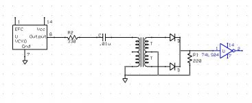
Here is a first pass. The principle is to generate a positive edge on each transition. At low frequencies this won't work but at 50 MHz the source rise time is slow enough to make for more of a triangle wave than a perfect square wave. I would breadboard it before committing to a layout.
First, Minicircuits has many well suited transformers and they are pretty reasonably priced. Second, use Shottky diodes, there is no signal or transition time to waste. The capacitance is low and the phase noise will be lower. Third, getting the gate to switch will be the challenge and may need tweaking. For a 100 MHz output you will need a fast scope to see what is happening and very good technique to see it well. No long ground leads. Use a sampling scope if you have one. The period on the output will be 10 nS or a transition every 5 nS. The gate on the output should be 74AC04 and well bypassed.
Thanks Demian, that a very interesting idea. I like the passive design. Will try it once I get time.
Regards,
Ian
Hi AR2
Your projects are beautiful, where did you buy all those nice connectors (USB, coaxial) and the case? Are you panels done by Front panel express?
Thank you bigpandahk,
Some I purchased from Mouser, you are probably referring to the Neutric USB connector. That one is really nice one, Mouser sells them. Check Neutric site for full selection. On my cases, I machined panels and sent out for anodizing. The other one is older Proceed case that I gutted out to house all my digital electronics.
Best
AR2
Run 22.5792Mhz or a 24.5760Mhz XO (CCHD-957) on single XO Clock Board
Hi Gary,
With FIFO FW V3.80 or higher, you can use a 22.5792Mhz or a 24.5760Mhz XO (CCHD-957) directly from the socket on the single XO clock board, please refer to the technical documents at bottom of the GB II post for setting the jumpers.
The sinale XO clock board could provide up to 150mA 3.3V power for the XO socket, but I don't think you need making any additional adapter .
Please let me know for any question.
Regards,
Ian
Hi Gary,
With FIFO FW V3.80 or higher, you can use a 22.5792Mhz or a 24.5760Mhz XO (CCHD-957) directly from the socket on the single XO clock board, please refer to the technical documents at bottom of the GB II post for setting the jumpers.
The sinale XO clock board could provide up to 150mA 3.3V power for the XO socket, but I don't think you need making any additional adapter
.Please let me know for any question.
Regards,
Ian
Ian,
Thanks for your quick reply in a very busy time for you.
I'd like to get an improved 11.2896M XO clock using the single board. If I want to use the CCHD-957 I need to make very small adapter PCB with a 74ACH74 to divide it by 2 to get my target frequency for the TDA1541A.
It will be small enough with pins back in the right place to plug directly into the socket. The available current will certainly be adequate to supply the flip-flop. Since I also do PCB layout, making it will be pretty straightforward.
Ian, any other options to get a high(er) performance 11.2896M clock signal?
Regards,
Gary
Hi Gary,
With FIFO FW V3.80 or higher, you can use a 22.5792Mhz or a 24.5760Mhz XO (CCHD-957) directly from the socket on the single XO clock board, please refer to the technical documents at bottom of the GB II post for setting the jumpers.
The sinale XO clock board could provide up to 150mA 3.3V power for the XO socket, but I don't think you need making any additional adapter
Please let me know for any question.
Regards,
Ian
Ian,
Thanks for your quick reply in a very busy time for you.
I'd like to get an improved 11.2896M XO clock using the single board. If I want to use the CCHD-957 I need to make very small adapter PCB with a 74ACH74 to divide it by 2 to get my target frequency for the TDA1541A.
It will be small enough with pins back in the right place to plug directly into the socket. The available current will certainly be adequate to supply the flip-flop. Since I also do PCB layout, making it will be pretty straightforward.
Ian, any other options to get a high(er) performance 11.2896M clock signal?
Regards,
Gary
Yes,it's true, it's very hard to find a nice 11.2896Mhz clock. Actually the ppm is not that important, but the phase noise really affects the sound quality, both close-in and noise floor are. Power supply as well.
I did try quite a few 11.2896 XOs, the best one so far I tested was Si570.But the close-in phase noise is still not as good as CCHD-957 according to the specifications. Unfortunately Crystek doesn't have a 11.2896 one.
Making an adapter is a good idea. You may compare 74ACH74 and PO74G74 GHz TTL from Potato to see which one is better as a /2 divider. I'm interested in your progress, please let me know the result.
Regards,
Ian
Ian,
Will do. I'm not certain there should be any noise contribution from dividing the clock down - since phase noise is generated through a source. I'll check out the PO74G74 first.
I will share the PCB layout, or make available to anyone in the forum; or even have some of these "micro-pcb's" made if there is interest. However, I'll send it to you to let you verify it and give it you OK to use with your single clock board before I do that.
Regards,
Gary
Yes,it's true, it's very hard to find a nice 11.2896Mhz clock. Actually the ppm is not that important, but the phase noise really affects the sound quality, both close-in and noise floor are. Power supply as well.
I did try quite a few 11.2896 XOs, the best one so far I tested was Si570.But the close-in phase noise is still not as good as CCHD-957 according to the specifications. Unfortunately Crystek doesn't have a 11.2896 one.
Making an adapter is a good idea. You may compare 74ACH74 and PO74G74 GHz TTL from Potato to see which one is better as a /2 divider. I'm interested in your progress, please let me know the result.
Regards,
Ian
Gary,
The 11.29 clock, as I want to use with a tda1541 as well, does it need to be 5 volt too? As I understood the FIFO could plug and talk directly to tda1541 until I was reading about the daughter board requirements.
Can it please be confirmed what extra is req to run this on a tda1541 please.
Thanks,
Drew.
Gary,
The 11.29 clock, as I want to use with a tda1541 as well, does it need to be 5 volt too? As I understood the FIFO could plug and talk directly to tda1541 until I was reading about the daughter board requirements.
Can it please be confirmed what extra is req to run this on a tda1541 please.
Thanks,
Drew.
Sorry to the thread users, this response is a bit off topic.
There's a fair bit of discussion about the exact level of drive on the clock signal on the TDA1541A that's appropriate. Check this long running thread:
http://www.diyaudio.com/forums/digi...building-ultimate-nos-dac-using-tda1541a.html
I'm presently running the I2S signals in at about 3.5V with no problem at all, and will still try a bit of experimentation as per the many posts in that thread about drive levels. The short of it is that TTL needs at least 2V to be considered a logic HIGH (but really need to be higher for noise margin), so you should be OK with Ian's board.
Noise margin = Voh (drive) - Vih (input min) = 3.5 -2.0 = 1.5V
Gary
Last edited:
R&D progress, Si570 based clock board, first prototype
The first prototype of Si570 based clock board was down. With the single programmable XO, now I got 11.2896, 12.2880, 16.9344, 18.4320, 22.5792, 24.5760, 33.8688, 45.1584, 49.1520, 90.3168, 98.3040 MHz. Switching between frequencies will take only a couple of ms. Pretty amazing for such a small gear.
This Si570 based clock board could be a universal digital audio clock generator/FIFO clock board/ESS9018 sync mode clock board (90.xxx and 98.xxx).
FW driver was down. Hardware still need some revising to support 2048*Fs with perfect on current V3.80 FIFO FW.
Ian
Attachments
The first prototype of Si570 based clock board was down. With the single programmable XO, now I got 11.2896, 12.2880, 16.9344, 18.4320, 22.5792, 24.5760, 33.8688, 45.1584, 49.1520, 90.3168, 98.3040 MHz. Switching between frequencies will take only a couple of ms. Pretty amazing for such a small gear.
This Si570 based clock board could be a universal digital audio clock generator/FIFO clock board/ESS9018 sync mode clock board (90.xxx and 98.xxx).
FW driver was down. Hardware still need some revising to support 2048*Fs with perfect on current V3.80 FIFO FW.
Ian
Nice! With the programmable SiLabs XO, what phase noise are you expecting to get? Probably nowhere near the Crystek, but perhaps better than the run-of-the-mill XO's?
.........Si570....... CCHD957
10- Hz N/A .........-97dB
100Hz -112dB ....-126dB
1-KHz -122dB ....-148dB
10KHz -132dB ....-162dB
100KHz -137dB ...-171dB
1-Mhz -144dB .....-170dB
10Mhz -150dB ......N/A
100Mhz N/A .........N/A
Excellent numbers. I think the versatility of this board would be an equitable trade for the difference in phase noise. Those numbers certainly better than any of the typical 11.2M XO's.

- Home
- Source & Line
- Digital Line Level
- Asynchronous I2S FIFO project, an ultimate weapon to fight the jitter