You remind me of a certain type of politician. They are never wrong, simply not understood. Faced with that, there is nothing more to be said.
Politic it's not allowed on this forum.
It's a real shame but I can't get into the subject.
Time will tell if I'm wrong.
Surely you are not wrong, since your contribution to this diy forum is rather limited.
I don't remember any of your designs, but maybe I'm not well up to date.
As expected; FYI, the English language has plenty of colloquial phrases and idioms. Instead of your regular knee jerk reactions, you could first check what is your peer trying to say. A few point in case references:
Everybody and their dog - Idioms by The Free Dictionary
everybody and their dog
everyone and their dog - Wiktionary
Everybody-and-their-dog Meaning | Best 1 Definitions of Everybody-and-their-dog
Yes, this is a big insult.
Sorry, but although I'm not mother tongue and so I'm not here to teach English literature, there is no doubts about this idioms
Urban Dictionary: anyone with half a brain
And, of course, an ASRC with it's PLL is deemed insufficiant.
It's funny to see how, while strongly suggesting that a PLL is an inferior solution for cleaning the clock jitter, and something like your low phase noise clock is so much better, you are at the same time willing to accept the ES9038 internal ASRC with it's DPLL.
Syn, I think the DPLL's jitter rejection corner freq is adjustable down to 0.1Hz.
If this is the case it should retain the possible benefits of sub 10Hz UL phase
noise clock. Whether those benefits actually exist has been covered.
TCD
At zero crossing all the switches of the DAC change theirs state (eg. from 00000000000000000000 to 11111111111111111111), this could cause the glitch.
I wonder why your former fellows have not implemented the sign magnitude DAC operation which could solve the glitch issue.
Read the data sheet, this part is not for audio.
Is the internal clock accessible externally? You could build a phase noise detector with it if so. Or access the control to the Vic as an indicator. Not sure what you would learn other than its noise is higher than most reference clocks.Syn, I think the DPLL's jitter rejection corner freq is adjustable down to 0.1Hz.
If this is the case it should retain the possible benefits of sub 10Hz UL phase
noise clock. Whether those benefits actually exist has been covered.
TCD
Read the data sheet, this part is not for audio.
I have read the data sheet, I know that audio is not specified between the applications.
Anyway I don't see any disadvantage using sign magnitude architecture such as the PCM1704, I see only advantages even for industrial applications.
Moreover, even if the DAC is not specified for audio use, IMHO it does not mean that it cannot be used in audio applications.
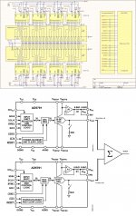
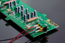
Is the DAC in the upper part of the attached picture suitable for audio applications?
If so, I don't see much difference than the DAC at the bottom of the picture.
Attachments
You clearly don't understand the business, twice the silicon for all customers even if they don't need it. Let the few 1000 audiophiles that still want to play with multi-bit DAC's buy four or as mentioned design an external de-glitcher. It's been done and the results are remarkable, maybe you are up for it.
Last edited:
You clearly don't understand the business, twice the silicon for all customers even if they don't need it. Let the few 1000 audiophiles that still want to play with multi-bit DAC's buy four or as mentioned design an external de-glitcher. It's been done and the results are remarkable, maybe you are up for it.
Although Management & Control, Costing, Business Process are just a part of my current job as a consultant (syn08 has linked my Linkedin profile several times) I have to admit I don't know the detail of a multi-bit DAC manufacturing process.
I would curious to know what twice the silicon means in costing term.
Can you share your experience about fixed and variables costs of such manufacturing process (from the design to the end of life)?
I can help you with that, although my information could be outdated, there are 30 years since I was working in a semiconductor plant. At the time, we were using a variant of the Seeds model, known as the Bose-Einstein model. As such, the die yield when doubling the chip area could be estimated with a high confidence level as Y2=Y1[(1+A1*D)/(1+A2*D)^n where
Y2 is the wafer level yield of a chip of area A2 cm^2
Y1 is the wafer level yield of a chip of area A1 cm^2
D is the average killing defect number per cm^2
n is the number of process critical mask levels
So the result strongly depends on the general cleanliness of the manufacturing line D and the number of critical masks n. Taking some random numbers, assume Y1= 75% A2=0.2 cm^2 A1=0.1 cm^2 D= 0.25 cm^-2 and n=14 we get Y2=53%
In a very simplified model, the cost of the Y2 chip will be twice the cost of the Y1 chip (you get half the chips on each wafer, due to the double area) multiplied by the yield ratios, which is 75/53. If the Y1 chip price is $1, a chip double in area will cost $2.8
This is a very rough yield model, good for an initial estimate. The wafer reality could be +/-25% (at least that's what we got in practice, at the time). I recall the larger the chip areas were, the more pessimistic the evaluation was, statistical reason being you could have more than one killing defect per chip, so for a fixed D value the yield was, from a certain area up, no longer scaling linearly with the chip area.
I can help you with that, although my information could be outdated, there are 30 years since I was working in a semiconductor plant. At the time, we were using a variant of the Seeds model, known as the Bose-Einstein model. As such, the die yield when doubling the chip area could be estimated with a high confidence level as Y2=Y1[(1+A1*D)/(1+A2*D)^n where
Y2 is the wafer level yield of a chip of area A2 cm^2
Y1 is the wafer level yield of a chip of area A1 cm^2
D is the average killing defect number per cm^2
n is the number of process critical mask levels
So the result strongly depends on the general cleanliness of the manufacturing line D and the number of critical masks n. Taking some random numbers, assume Y1= 75% A2=0.2 cm^2 A1=0.1 cm^2 D= 0.25 cm^-2 and n=14 we get Y2=53%
In a very simplified model, the cost of the Y2 chip will be twice the cost of the Y1 chip (you get half the chips on each wafer, due to the double area) multiplied by the yield ratios, which is 75/53. If the Y1 chip price is $1, a chip double in area will cost $2.8
This is a very rough yield model, good for an initial estimate. The wafer reality could be +/-25% (at least that's what we got in practice, at the time). I recall the larger the chip areas were, the more pessimistic the evaluation was, statistical reason being you could have more than one killing defect per chip, so for a fixed D value the yield was, from a certain area up, no longer scaling linearly with the chip area.
I have found this theses about process costing of CMOS microchip
https://core.ac.uk/download/pdf/230456504.pdf
Wafer cost is around 20% of the total cost.
Most of the calculated total cost are fixed costs.
This makes the determination of the product cost very uncertain as the final result will be heavily influenced by the distribution of fixed costs.
While direct costing process provides very reliable results, when the distribution of fixed costs is involved the result become uncertain and arbitrary, heavily dependent on the chosen cost drivers.
The distribution of fixed costs very often produces cross-subsidization errors that invalidate the determination of the product cost to the point of making it totally unreliable.
Activity Base Costing approach could help but it's very difficult to be applied and makes the choice of cost drivers even more critical.
Moreover we have no process and business data to be used so it all ends in pure speculation.
IMHO, doubling the DAC part of the chip does not mean doubling the wafer area, control logic and other parts remain almost the same.
You need 2 x 19 bit DAC instead of 1 x 20 bit DAC, wich means adding 90 resistors (64 for 6 bit thermometer decoded plus 26 for 13 bit R2R decoded), several active devices operating as switches and a little control logic.
I don't believe this means doubling the wafer area, I could estimate less than 50% more, maybe less.
Just for speculation we can assume a cost increasing about 10% (50% of 20%).
And just for speculation let assume a wafer cost of $3 per square inch or $ 0.00465 per square mm.
The AD5791 is a TSSOP-20 package device, 6.5 x 4.4 mm or 28.6 square mm, so the wafer cost would be $ 0.13299.
Finally a 50% wafer cost increasing means $ 0.0665 for a product sold at $ 113.53.
Now let me point to the FPGA we have used in our FIFO, the Xilinx XC3S200-4VQ100C.
It's a 63 I/O in VQFP-100 package, 16 x 16 mm and costs EUR 17.83.
Its big brother XC3S200-4TQG144C is a 97 I/O in TQFP-144 package, 22 x 22 mm and costs EUR 16.56.
Size ratio is 1.89 (89% bigger) and the unit price is the same.
Since we have no real costs data from the factory these are just speculations.
But this is not a business forum so this is just off topic, sorry.
Hello Norway,
As soon as my Sinepi has arrived i will start my own thread and hope that one will not be polluted like this one.
This thread wont go back to a normal one.
Greetings, eduard
Looking forward to it, eduard
Hello Norway,
I know Doede will receive a Sinepi soon and Ian promised me one of the first serie to be made after Doede's judgement.
BUT right now there is not much of a schedule for the circuit to arrive.
Maybe Doede will decide to publish the results in his own blog which is a lot more serious than diyaudio.com right now!
Greetings,Eduard
Trying to get the most out of TWTMC clocks for FifoPi (10)
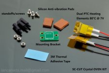
Oven solution for SC-Cut crystals
SC-Cut crystals need ovens at 80-90°C to achieve a better frequency stability. The temperature is pretty high. I’ve tried several solutions without success until I finalized this dual heating element PTC ceramic oven solution.
The PTC heating elements were customized at 80°C with 6.5-7VDC voltage. Increasing voltage can make the temperature higher a little bit but not by too much. Each heater will consume around 250mA current before warm up so a dual oven will need 0.5A. A LinearPi configured to 7V would be a very good power supply to drive the ovens. Low EMI noise power supplies are preferred. Please don’t use SMPS to avoid introducing EMI into the OCXO case.
I use a dual PTC heater configuration for the SC-Cut crystal to make the temperature evenly on both sides. It’s a better solution than the single heat element configuration.
The oven KIT will include:
2*PTC heat element
3M thermal conductive adhesive transfer tape
Silicone anti-vibration pads
Mount bracket
Standoffs / screws
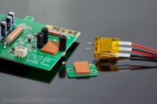
Drilling holes on the aluminum front panel of the Hammond case can result in shorting the isolated DRIXO output to ground. I designed a panel PCB with a double shield layer to fix the issue and to make things easier.
After installing this oven KIT to my DRIXO, it really made a change to the sound quality in my system. At the beginning, I didn’t feel any improvement. But after warm-up for more than 24 hours, the sound stage becomes more open. And then, after turning off the oven power for half an hour, it comes back again. I did this test back and forth a couple of times, the results are the same. But anyway, it is a subjective test. Different systems and different people may have different results. So, please just trust your ears.
Other links:
1.https://www.diyaudio.com/forums/dig...mate-weapon-fight-jitter-657.html#post6668751
2.https://www.diyaudio.com/forums/dig...mate-weapon-fight-jitter-660.html#post6671042
3.https://www.diyaudio.com/forums/dig...mate-weapon-fight-jitter-662.html#post6675622
4.https://www.diyaudio.com/forums/dig...mate-weapon-fight-jitter-664.html#post6678025
5.https://www.diyaudio.com/forums/dig...mate-weapon-fight-jitter-673.html#post6686256
6.https://www.diyaudio.com/forums/dig...mate-weapon-fight-jitter-677.html#post6690153
7.https://www.diyaudio.com/forums/dig...mate-weapon-fight-jitter-682.html#post6704886
8.https://www.diyaudio.com/forums/dig...mate-weapon-fight-jitter-687.html#post6718041
9.https://www.diyaudio.com/forums/dig...mate-weapon-fight-jitter-694.html#post6741950
Ian
Oven solution for SC-Cut crystals
SC-Cut crystals need ovens at 80-90°C to achieve a better frequency stability. The temperature is pretty high. I’ve tried several solutions without success until I finalized this dual heating element PTC ceramic oven solution.
The PTC heating elements were customized at 80°C with 6.5-7VDC voltage. Increasing voltage can make the temperature higher a little bit but not by too much. Each heater will consume around 250mA current before warm up so a dual oven will need 0.5A. A LinearPi configured to 7V would be a very good power supply to drive the ovens. Low EMI noise power supplies are preferred. Please don’t use SMPS to avoid introducing EMI into the OCXO case.
I use a dual PTC heater configuration for the SC-Cut crystal to make the temperature evenly on both sides. It’s a better solution than the single heat element configuration.
The oven KIT will include:
2*PTC heat element
3M thermal conductive adhesive transfer tape
Silicone anti-vibration pads
Mount bracket
Standoffs / screws
Drilling holes on the aluminum front panel of the Hammond case can result in shorting the isolated DRIXO output to ground. I designed a panel PCB with a double shield layer to fix the issue and to make things easier.
After installing this oven KIT to my DRIXO, it really made a change to the sound quality in my system. At the beginning, I didn’t feel any improvement. But after warm-up for more than 24 hours, the sound stage becomes more open. And then, after turning off the oven power for half an hour, it comes back again. I did this test back and forth a couple of times, the results are the same. But anyway, it is a subjective test. Different systems and different people may have different results. So, please just trust your ears.
Other links:
1.https://www.diyaudio.com/forums/dig...mate-weapon-fight-jitter-657.html#post6668751
2.https://www.diyaudio.com/forums/dig...mate-weapon-fight-jitter-660.html#post6671042
3.https://www.diyaudio.com/forums/dig...mate-weapon-fight-jitter-662.html#post6675622
4.https://www.diyaudio.com/forums/dig...mate-weapon-fight-jitter-664.html#post6678025
5.https://www.diyaudio.com/forums/dig...mate-weapon-fight-jitter-673.html#post6686256
6.https://www.diyaudio.com/forums/dig...mate-weapon-fight-jitter-677.html#post6690153
7.https://www.diyaudio.com/forums/dig...mate-weapon-fight-jitter-682.html#post6704886
8.https://www.diyaudio.com/forums/dig...mate-weapon-fight-jitter-687.html#post6718041
9.https://www.diyaudio.com/forums/dig...mate-weapon-fight-jitter-694.html#post6741950
Ian
Attachments
Last edited:
Hello Ian,
Before there is any "" customer " who has a Sinepi at home which is actually working you will surprise us with yet another thing that we need to get to reach audio nirvana.
Wouldn't it be MUCH better to " publish " an improvement with bigger intervals. To ME it doesnt feel comfortable.
OR write about something to improve sound that wont require a weekly salary investment.
Hypoglycemia, Eduard
Hey eduard, you do not need to buy every one.")
I actually think this is an interesting development as no one else other than Andrea experimented with a heating element on the 5MHz SC cut crystal. I thought about getting a cheap ebay usb heating pad to run the experiment. That remains an option, or if Ian creates a kit that addresses heating and vibration it may be an attractive option. I like that someone is working to push the boundary of this thing.
Surely this could operate from a surplus wall wart phone charger? Is there any issue that would not equally created by another wall wart to power say the network router that may be on the same circuit? I realize your system is running on a Power Plant. Have you tried powering the heater with a switching PS that is outside the Power Plant domain?
@Wlowes,
PTC ceramic heating elements are self-feedback components. The temperature is decided. Temperature is not sensitive to the voltage of power supply. So I don't think the quality the power supply is really matter for the PTC. The only thing I'm concerned about the the possible EMI noise. Because they will be installed very closed to the Sc-cut crystal.
As long as the heater power has an independent/isolated coil, I don't think it needs the Power Plant domain. Or, you can try it by yourself. Hopefully I could make this OVEN KIT available together with the SinePi.
Regards,
Ian
- Home
- Source & Line
- Digital Line Level
- Asynchronous I2S FIFO project, an ultimate weapon to fight the jitter