In the DIY community, the development effort is usually not amortized into individual units, which makes the part cost the primary concern. Having a low total part cost would just benefit everyone, right?
My answer will be yes and no, yes because you are right, no because in lan's design, I think the clock section cost should be more critical and much expensive then SRAM.
My answer will be yes and no, yes because you are right, no because in lan's design, I think the clock section cost should be more critical and much expensive then SRAM.
But again feeding this CPLD/FPGA a high quality clock really won't improve thiings a lot. These chips have intrinsic jitter that you can't get away from and low jitter clock will be swamped. Use a high quality clock to feed the FPGA and also so you can reclock its I2S output, then your jitter levels will be near equal the clock, probably the lowest jitter device I have seen directly prior to the DAC chip, but again only if reclocked to remove the intrinsic jitter.
No we have your FIFO, feeding your chip a high quality clock, great now we have jitter equal to intrisic jitter of the FIFO chip + clock jitter. Now I'll bet a few dollars the chip used here has more intrinsic jitter than a 9001 which was specifically layed out for digital audio. So I guess what I am saying is if your transport is very good, your FIFO will probably add overall jitter.
Solution is easy, simply reclock the output with the same crystal, this will eliminate the FIFO's potentially high intrinsic jitter. This technique has been used for years dealing with CD decoders, it works and should be considered here.
If you look closely at the picture, the local master clock doe not 'pass' the FIFO chip. It is feeding both the FIFO chip and the DAC chip at the same time. Unless your DAC chip is sensitive to jitter on signals other than the master clock (i.e. BCLK, LRCK, DATA), it would not be necessary to reclock them. Even if we choose to reclock the signals, the output registers at the pad of the FIFO chip does not necessarily perform worse than an LVCMOS logic chip, which means reclocking internally would be good enough. Price is not a reliable indication of the performance of a chip.
Very good question, Guido. I'm afraid if the FIFO is empty, it will sound like repeating a word(around 1s for 44.K), and when it full, it will sound like short a word(around 1s for 44.K). Meanwhile, no pause,silence and other noise. Just imagine if you have a cassette, cut 1secnd length or extend it with 1 second copy, would be the same thing as FIFO full and empty.
When you play the continue live concerts, this will happen every couple of hours if the sampling clock is not that bad(with 100ppm frequency tolerance).
PLL is another solution. According to my quite limited knowledge on this issue, the key thing should the bandwidth. If you reduce that bandwidth to a certain level, you might still need a FIFO to buffer the data, but may not that big ...
Maybe I'm wrong or you have some good idea..anyway, good luck to your project. Have a good night. Ian
Sounds the same as what happens when you put an 8416 in slave mode; it skips or doubles samples (at a higher rate). So when you run full/empty, you "reset" to the other opposite; emtying or filling the memory (get the max time between the occurences)? But the frequency of such event would all depend on the sampling rate i guess.
PLL.. My knowledge is also limited
") But i had some help on the way. You do need a FIFO, but with depth of one. So the one in the 8416 is good enough. Getting a good masterclock out of a VCXO is the challenge here.
But i had some help on the way. You do need a FIFO, but with depth of one. So the one in the 8416 is good enough. Getting a good masterclock out of a VCXO is the challenge here.Need to pick it up again.
I did use a small async fifo once to decouple some clock domains. But that was with one clock distributed into a cd player. With easy control; start the readout at half-full.
I have a timing analyser to do some basic jitter measurements. But it's an old beast. Let's say i see the difference between a good and a bad clock
I have a timing analyser to do some basic jitter measurements. But it's an old beast. Let's say i see the difference between a good and a bad clock
Very cool, Guido. What type is that 'old beast'? Did you find any really nice clock?
BTW. I like your logo. Me too a swing arm laser pickup fan.
) Ian.
Last edited:
Kode Odetics 3100
Very old PC AT or XT with hercules card/monitor and specific hardware...
I did compared some spdif sources at the output of a receiver (picture), compared a decent clock with the 7220 output etc. I'm using tent clocks mainly, but that is more the good availability for me. With it's resolution it is really comparing good clock/bad clock.
As for pll development, you can set it on a reduced number of counts (10000 or so) and on repeat. Then you can see the clock dancing on the noise getting into the VCXO (need to make a pcb before i can continue with the software).
An externally hosted image should be here but it was not working when we last tested it.
Very old
PC AT or XT with hercules card/monitor and specific hardware...I did compared some spdif sources at the output of a receiver (picture), compared a decent clock with the 7220 output etc. I'm using tent clocks mainly, but that is more the good availability for me. With it's resolution it is really comparing good clock/bad clock.
As for pll development, you can set it on a reduced number of counts (10000 or so) and on repeat. Then you can see the clock dancing on the noise getting into the VCXO (need to make a pcb before i can continue with the software).
Last edited:
Amazing, Guido. It's old but it's working! What is the principle of this Kode 3100? It measure the jitter from frequency domain or from time domain? It seems it's measuring the RMS period jitter, right? What is the minimal resolution of it in ps? What is the background noise or tolorance? I'm still trying to find out the car price toy with jitter measurement package from universities or labs around GTA area for my project. Very impressed. Nice weekend. IanKode Odetics 3100.
The beast with more old boatanchors.
Errr. I just compare I wouldn't dare read numbers; this thing missed calibration for a long time. Resolution is 0.1 nSec.
It shows counts; it has 4000 memory locations. from the input you start a counter on a rising edge and you stop on the next rising edge. Threshold can be set (values match for 1:10 probe). So when it's stopped you have a counter value, say 3345. Now you take memory location 3345, get the value, add one and store back in memory. Then do this a lot of times 10^8 or so. In the end you have a value in memory location 3345, but also in 3444, 3446 etc. This is plotted on the screen as a histogram. horizontal the 4000 memory locations (optionally a 2 or 5 zoom). Vertical is the number of occurences, logarithmic scale. So i would say, it measures from the time domain.
You can calculate an average, stable or exponential. You get a number in seconds as standard deviation from the main time.
To increase resolution, you can set a delay between the start edge and the start of the counter. So you can "zoom in".
Also you can measure more than a clock. E.g. the output of a bitstream dac has 6 different time intervals iirc. You can segment the output into sections and then do the maths over all sections.
Think it was expensive in the days, but i got it for about a 100 usd. Danger is if something breaks, i won't be able to fix as it's a lot of ttl inside and no service manual. And the monitor part is not reliable. But modern ones are quite expensive.
Note in the first picture, the clock with the widest jitterspectrum actually has the lower standard deviation. I don't know which one would be better....
But please, back to your work. It's more interesting.
If you want me to do some measurements, please send a spare board
An externally hosted image should be here but it was not working when we last tested it.
Errr. I just compare
I wouldn't dare read numbers; this thing missed calibration for a long time. Resolution is 0.1 nSec.It shows counts; it has 4000 memory locations. from the input you start a counter on a rising edge and you stop on the next rising edge. Threshold can be set (values match for 1:10 probe). So when it's stopped you have a counter value, say 3345. Now you take memory location 3345, get the value, add one and store back in memory. Then do this a lot of times 10^8 or so. In the end you have a value in memory location 3345, but also in 3444, 3446 etc. This is plotted on the screen as a histogram. horizontal the 4000 memory locations (optionally a 2 or 5 zoom). Vertical is the number of occurences, logarithmic scale. So i would say, it measures from the time domain.
You can calculate an average, stable or exponential. You get a number in seconds as standard deviation from the main time.
To increase resolution, you can set a delay between the start edge and the start of the counter. So you can "zoom in".
Also you can measure more than a clock. E.g. the output of a bitstream dac has 6 different time intervals iirc. You can segment the output into sections and then do the maths over all sections.
Think it was expensive in the days, but i got it for about a 100 usd. Danger is if something breaks, i won't be able to fix as it's a lot of ttl inside and no service manual. And the monitor part is not reliable. But modern ones are quite expensive.
Note in the first picture, the clock with the widest jitterspectrum actually has the lower standard deviation. I don't know which one would be better....
But please, back to your work. It's more interesting.
If you want me to do some measurements, please send a spare board
Last edited:
For the most 'fun-factor', a FIFO board would be BYOC (bring your own clock).
Using an SMA tee connector on the clock line seems to indicate that you are not an RF engineer
Hi Simmconn, You are very smart guy; it seems you know all the gear. Thanks. Yes, you are right; I noticed the SMA tee problem. For the 8” cable, the first reflection comes back just at the moment of the middle of the raising edge of the MCLK (1.73ns later, the signal velocity in that 50ohm cable is around 0.77C), and so on the second, the third… Those reflections may tribute more jitter to the MCLK. To avoid this, on the clock boards I am doing right now I have standalone path to feed the clock to the FIFO, and the MCLK will output to the DAC directly from the clock board point to point without any branch via the coaxial cable after the impedance match.
I hope I was a RF engineer from a telecommunication company. So that, I could design the magic clock oscillator together with deep theories and equations posting on the thread to make everybody believe in J. But, unfortunately I am just an average person and don’t have the ability to make that ‘magic’. So, in this FIFO project, I would keep the clock oscillator as an open concept. That means the clock will be replaceable and upgradeable. No matter what kind of clock I have, I could make use of it for my FIFO. Just as you side: “a FIFO board would be BYOC (bring your own clock)”. And I would like to add a word: bring more fun!
According to my limited understanding on the jitter principle, working together with a DAC, the clock just behaves like a filter. Two clocks even they have the similar jitter level, they may sound different because of the difference on the jitter spectrum and characteristics. Things are quite similar to the vacuum tubes. Two ECC83 tubes, for example, one from Telefunken another from Mullard, they may have very closed testing results from a tube tester, but for sure, they sound different.
Keep bringing the funJ. Have a nice weekend. Ian
Last edited:
Consider the intrinsic jitter of any complex chip you are using. In this design say we have an incredible transport with documented 3ps jitter delivered to the DIR9001. After the DIR9001 we will have 53ps (+- based on the mckl per the datasheet), this intrinsic jitter is always added and has nothing to do with the corner frequency, above the corner frequency is where the 3ps from the transport will be passed (worst case).
No we have your FIFO, feeding your chip a high quality clock, great now we have jitter equal to intrisic jitter of the FIFO chip + clock jitter. Now I'll bet a few dollars the chip used here has more intrinsic jitter than a 9001 which was specifically layed out for digital audio. So I guess what I am saying is if your transport is very good, your FIFO will probably add overall jitter.
Solution is easy, simply reclock the output with the same crystal, this will eliminate the FIFO's potentially high intrinsic jitter. This technique has been used for years dealing with CD decoders, it works and should be considered here.
Hi Regal, I’m sorry for the delay of replying your post. I bet didn’t lose your dollars!
First, on the reclock issue, I agree with you. Because for those NOS DACs such as TAD1541, they don’t use MCLK for the internal timing, instead, they use SCK and WS driving the internal state machine. That means those NOS DACs are sensitive to the jitter on the signals other than the MCLK. In this case, reclock the I2S signal by the same master clock is a very good idea. And after doing that, the total jitter on the I2S signal=master clock jitter + additive jitter of the reclocking flip-flop. At is meaning, just as you said, the intrinsic jitter of FIFO was eliminated. But instead, the new flip-flop jitter is introduced.
On those clock boards I’m cooking right now for my FIFO project, the reclock circuits have already been included. The only thing is we need select the flip-flop with careful. Normally the flip-flops will also introduce quite a few amount of additive jitter. The best flip-flop is the PECL series, which the additive jitter is just around 1 ps level, unbelievable! The normal TTL or LVTTL flip-flop have the similar or little bit worse jitter level than the CPLD on the FIFO board. Some new generation flip-flops, such as AUP, AUC series, have better jitter performance. I’m not recommended using the S,AS,F series TTL IC doing the reclock job, not only because the speed is not as good as the new technologies, but also, the high switching current will introduce big ripple on the power supply which will increase the clock jitter rapidly.
On the FIFO issues, the FIFO isolates the two clock domain. For example, you have a FIFO and a reclock circuit between the DIR9001 and your DAC, the DIR9001 has 53ps jitter output on all signals, and the new low jitter clock has 10ps jitter, the reclock flip-flop has 20ps additive jitter. So, the result is: You get MCLK with 10ps jitter (MCLK output directly from clock board without passing the FIFO), and you get 30ps jitter on I2S signals other than MCLK after reclock. (All the jitter should be the RMS period jitter in the above example) .
The reclock topics are very interesting. If have chance, I would be very happy to discuss with you with details. Nice weekend. Ian
Feeling the jitter, my terrible experience
After got this I2S FIFO working, the first thing I couldn’t help to do was experiencing the ‘known’ jitter, although finally it approved the feeling was very bad. So at here, I just don’t suggest doing this kind of meaningless job anymore.
People did a lot of research about how the jitter should sound like and we could also find out the simulation results, the equations, and the spectrum plots from websites connected to this issue. So roughly I know how it would be.
I just came across having an IDT 5V9885 clock generator board for my previous FPGA projects. This clock board is not suitable for digital audio application because it comes with 200ps peak-to-peak period jitter; it was developed originally for FPGA design verification because it has three internal programmable PLLs. The only reason I want to use it was because on chip it integrated a programmable spread spectrum generation function, which means I could generate the ‘know’ jitter by programming the SSC.
The first step I did was programming the 5V9885 to generate an 11.2986MHz clock without SSC from CLK2 and connected it into my system by replacing the clock board I had before. Again, I use battery power this 5V9885 board to exclude the influence of the power supply. It sounds OK, same level as the analog output quality of a hundred bucks DVD player and worse than the direct I2S and MCLK output from DIR9001.
And then, I programmed the SSC to generate the same frequency clock but with +-200ps period jitter with 2KHz modulation. When I turned it on, I was totally shocked. The sound was so bad; I never thought my B&W 804 speakers could sound horrible like that. Everything was mixed up at background and I couldn’t distinguish the positions of the singer and the instruments. It was noisy and without any details. I lost the focus, lost the depth, lost the 3D feelings. After a while, I got a bit sick and my ears were very uncomfortable. So I stopped this research which I thought I could go deeper. When I switched it back to DIR9001, I found it still sound bad. I started to suspect something wrong with my system. But finally I realize it was something wrong with my listening and it didn’t recover until hours later.
That terrible experience was almost killing my motivation to continue my hobby of audio DIY and making I feel bad, so I decided not to do this kind of evaluation any more. Although my jitter experiencing testing is not a typical case and that kind of jitter may not exist in the real world of digital audio, but at least it confirmed what they said about how the jitter should sounds like was true.
I think I really need doing something nice to make me feel better, for example, finding out the beauty from clocksJ.
Attachments
thats a cool story and yes i think i have experienced a similar situation on occasion. basically it removes any specificity to the imaging, which on headphones is quite disorienting. thats a very interesting looking board, can you tell me more?
Hi Qusp, That clock board was just an IDT 5V9885 EVB, nothing special. You can download all the docs and softwares from IDT - Integrated Device Technology - EEPROM Reprogrammable > 5V9885C . 5V9885 is not a most updated programmable clock generator. But the good thing is you can generate any frequency you want. That is a very usefull feature for testing the boards. For example, your can generate the master clock for different Fs and get your board go through all the case. We can find something even better from TI or AD now.
I still can't come back to the job of coding and testing the FIFO clock board which was almost finished. Hopefully I could show you something on the weekend. Ian
Last edited:
Hi guys, I’m coming back.
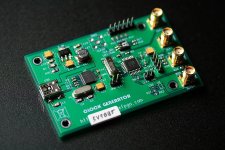
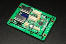
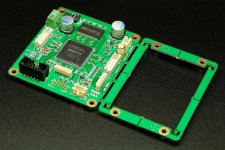
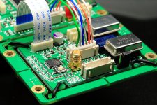
I just could be able to show you the first clock board I designed for this FIFO project: the Double XO Clock Board. Please see the attached pictures.
The features are as below:
1. Frequency supported
44.1KHz 16bit (24bit/32bit ready)
48KHz 16bit (24bit/32bit ready)
88.2KHz 16bit/24bit (32bit ready)
96KHz 16bit/24bit (32bit ready)
176.4KHz 16bit/24bit/32bit
192KHz 16bit/24bit/32bit
2. Switching the MCLK and *Fs automatically according to the input I2S stream;
3. XO options for the socket U1:
11.2896MHz (go 44.1K and 88.2K)
Or, 22.5792MHz (go 44.1K, 88.2K and 176.4K)
14Pin or 9Pin standard XO with 3.3V Vcc
XO options for the socket U2:
12.2880MHz (go 48K and 96K)
Or, 24.5760MHz (go 48K, 96K and 192K)
14Pin or 9Pin standard XO with 3.3V Vcc
4. Re-clock function was equipped on board;
5. Manual frequency switching button for optional standalone working mode;
6. Output the MCLK and I2S signals directly without passing through FIFO;
7. Implement a relay for frequency switching to avoid any additive jitter from buffering the MCLK;
8. Frequency settings will be saved and applied automatically at next power up.
The FIFO board was designed having an optional frame connected which is compatible with the frame on the clock board(this idea just make the FIFO board could be easily integrated with different clock solution). We can pick up the clock board from its original frame by a side cutter, and hook it up to the FIFO board by four rubber rings to make them linked together as a whole piece; or, we could cut the frame from the FIFO board and make the FIFO and the clock board located separately. It’s quite flexible at this point. The purpose of using those rubber rings is to reduce the mechanical vibration which could also introduce the jitter into the XO output.
Interface with the FIFO board, basically only a 10 pin FFC cable is needed. If we want to use the re-clock function on the clock board, an additional I2S bridge cable will be connected. That’s all, nothing else, very easy.
This double XO clock board has a frequency management MCU. During normal operation, this MCU will run at deep sleep mode, or power down mode. In this mode, all of the clocks, include CPU clock, IO clock and watchdog clock, are stopped. That means the MCU do not generate any EMI noise at this time. When the frequency detecting logic on the FIFO board found input I2S frequency was changed, it will wake up the MCU by pulling down the interrupt line, and at same time silence the I2S output. After the wakeup, the MCU will set a new MCLK frequency as well as the *Fs according to the information provided by the FIFO board. Once the new frequency was set and confirmed good, the MCU will back to the deep sleep mode again.
There are nine LEDs on this clock board. Six of them are Fs frequency indicator to indicate six working Fs frequency (form 44.1 KHz to 192 KHz); Three of them are the *Fs indicator to indicate 128,256 or 512 *Fs.
This clock board, together with the FIFO board, are working very well with my system. The frequency switching function was amazing. For example, I’m playing a 44.1K APE by the foobar2000 player, and then I open a 96 KHz 24 bit APE file. The lock LED on the FIFO board will start flashing and the empty LED will turn on, after a while(around 2 seconds), I can hear a little click from the relay, and then the lock LED go solid, empty led turned off, the LEDs on the clock board new indicate 96Khz and 256Fs, and then the music starts. Very cool.
Again, both of the FIFO board and the clock board do not influence the sound quality (of cause they are bit perfect), what really decide the sound quality are the XOs which the clock board is equipped with. So, next step, the most important thing for me is looking for better clocks.
Enjoy the pictures. Ian
Attachments
-
 DoubleXOclockBoard1.JPG674.5 KB · Views: 3,279
 -
 DoubleXOclockBoard2.JPG648.6 KB · Views: 2,962
 -
 FIFOframe.JPG559.6 KB · Views: 2,836
 -
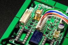 ReclockSection.JPG573.5 KB · Views: 1,264
 -
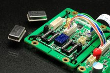 XOsockets.JPG573.3 KB · Views: 1,429
 -
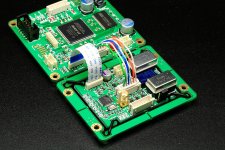 WorkWithFIFOboard.JPG679 KB · Views: 1,466
 -
 FrequencyIndicatorLEDs.JPG461.9 KB · Views: 1,448
Last edited:
So, next step, the most important thing for me is looking for better clocks.
I'd like to recommend;
CMOS output Crystal Clock Oscillator NZ2520SD
manufactured by a Japanese leading crystal maker, Nihon Dempa Kogyo Co., Ltd.;
NZ2520SD(OA / AV)/Crystal Clock Oscillators/NDK
http://www.ndk.com/images/products/catalog/c_NZ2520SD_NSA3449E_e.pdf
The model has a remarkable low phase noise profile. According to their measurement result sheet, Phase Noise [dBc/Hz] 26MHz 3.3V for 5 samples
1Hz: max -76, min -81
10Hz: max -108, min -111
100Hz: max -136, min -138
1kHz: max -151, min -152
10kHz: max -156, min -157
The component is also available for personal users by way of a Japanese online web store, chip1stop.
Chip One Stop - Shopping Site for Electronic Components and Semiconductors
The price I bought was 1,500 JPY / piece ( 20 USD/ piece )
and 1,000 JPY/10 pieces.
I'd like to recommend;
CMOS output Crystal Clock Oscillator NZ2520SD
manufactured by a Japanese leading crystal maker, Nihon Dempa Kogyo Co., Ltd.;
Thanks Bunpei. Thank you so much for those recommendations.
Very good XO with impressed phase noise performance, especially at the low range.
I'm gonna register a membership at that website and try to get the quotation. It seems both of 22.5792MHz and 24.5760Mhz, they don't keep in stock currentlly.
The only thing I'm concerned about is .. if it is available delivery to Canada.
I'll come back to you if I have more questions. Thanks again. Have a nice week. Ian
I designed a similar product several years ago, the Pace-Car. The difference is that the Pace-Car works in two synchronous modes and one asynchronous mode and does not overrun/underrun the FIFO. The one you designed is a lot like the Genesis Digital Lens, which had large enough FIFO to last through most CDs without under/overrun. The clock was old on the lens, so the jitter was not competitive with modern clocks. I thought about doing this initially, but with long playlists and computer audio becoming the favored method of playback, the over/underrun was inevitable.
You are definitely correct, that the clock is the most important part of this design, as all digital audio designs. In the past, I have sold upgrade clock options for all of my products using either Superclock4 or Ultraclock from Audiocominternational. The Ultraclock is the best sounding clock IMO, and that's probably why it commands $800 from Reference Audio Mods, the distributor. I charged the same when I offered it. I now have my own clock design, so I have discontinued use of Superclock4 and Ultraclock. The good news for you is that I still have some Ultraclocks in stock. I am willing to sell 2 Ultraclocks in any frequency you want for $700.00. These start with a fundamental crystal (not overtone) generating a sine-wave and then a fast comparator and buffer for the TTL output. I can confingure them for 5V or 3.3V output and any output impedance from 10 ohms to 110 ohms.
I have evaluated a lot of clocks over the last 12 years, and I can tell you that the only ones besides the Audiocom offerings that are interesting are expensive custom clocks which must be ordered in large quantities, usually 50 or 100 in each frequency, and they take some time to get. A minimum $1000 investment. Even once you get these, they must be powered with an excellent discrete regulator design to actually achieve low jitter. There are no guarantees that your design will deliver the specsheet jitter numbers.
This is why the Ultraclock is a nice alternative. It runs on 12VDC and has decent on-board op-amp based regulators and it just sounds good. Any frequency you need. Battery power to the 12VDC is even better.
if interested contact me at nugent@empiricalaudio.com
Steve N.
Empirical Audio
Last edited:
It looks like you took great effort to design the clock board. I do have a few comments:Hi guys, I’m coming back.
Enjoy the pictures. Ian
1) The clock switching based on input signal sample rate change should be instantaneous. Other than the time waiting for the incoming signal to be stable (to verify the sample rate change), there should be no need to wait for 2 seconds. Clearing the FIFO? The old data should be discarded anyway.
2) The CPLD should be able to generate all the control signals used to switch the oscillators. Having an MCU is nice but I don't see the necessity.
3) Using a relay to switch between clocks may not be a good idea. For starters, it is not glitch-free. That's probably why you use a separate controller because you need to reset the CPLD after the clock switching. Second, the regular relay is not suitable for clock switching. You would need the ones rated for GHz signals just to get the impedance control right - and they are not cheap.
I designed a similar product several years ago, the Pace-Car.
Hi Steve,
Thank you so much for sharing your design experience. I took a look at your website. You did some innovative products, very impressed. It seems we achieve the similar target by different direction. I roughly understand your method, very smart idea, I like it.
My solution is more direct, just a standard big enough FIFO with I2S interface. I noticed the ‘under/over run’ issue, so I developed a smart FIFO logic inside the FPGA, in most of the cases, it does not ‘under/over run’ neither, even having a long playlist from a computer based player.
Totally agree with you on the point of power supply. Yes, I found the clock circuit is very sensitive to the EMI noise introduced by the power supply.
My project is still undergoing and I’m gonna try different clock solutions later on. Thank you so much for the offer, just hope I could have chance try your famous Ultraclock meanwhile. I’ll take into consideration. Regards. Ian
1) The clock switching based on input signal sample rate change should be instantaneous. Other than the time waiting for the incoming signal to be stable (to verify the sample rate change), there should be no need to wait for 2 seconds. Clearing the FIFO? The old data should be discarded anyway.
2) The CPLD should be able to generate all the control signals used to switch the oscillators. Having an MCU is nice but I don't see the necessity.
3) Using a relay to switch between clocks may not be a good idea. For starters, it is not glitch-free. That's probably why you use a separate controller because you need to reset the CPLD after the clock switching. Second, the regular relay is not suitable for clock switching. You would need the ones rated for GHz signals just to get the impedance control right - and they are not cheap.
Hi Simmconn, Thank you so much for those comments. Appreciate. But at some of points, I’m afraid I couldn’t 100% agree with you. I think it was mainly because we keep the different idea on the I2S FIFO project design. I’d like to discuss with you.
If you took a close look at the pictures, you may find out, at the clock section, I have different design idea. My design idea on the clock board is kind of open concept. My FIFO board could not only compatible with the different XOs on this double XO clock board, but also expend different clock/timing solutions come together with different clock boards, such as PLL, DDS, synthesizer and other technologies. To achieve this function, I need set up a protocol between the FIFO and the clock board. According to same protocol, the MCU on different clock boards could perform the solution independent frequency management. That means, if I have a new clock technology five years later, I still could design a clock board at that time and make it working very well with today’s FIFO platform, because the protocol keeps no change. This advantage will show obviously on my subsequence clock board design. Comparing with the benefit it brought, that MCU is worth it. To keeping bring the ‘fun’, I’ll design series of clock boards, this is only the first one.
On the other hand, my I2S FIFO is working at slave mode; the clock board is the master device with highest priority. All of signals are generated by the clock board at finial stage in order to get the better jitter performance. I don’t think using a slave device to dominate the master frequency control is a good idea. Sorry, at this point, I couldn’t agree with you.
Talking about the relay, I couldn’t find anything more suitable for this double XO configuration other than it, unless you power and run the two XOs at same time which is the way I don’t like. Comparing with FPGA and other logic switching circuit, to switch between clocks, the relay almost introduces no additive jitter. That was the reason I use it. Yes you are right, some of the relays may not suitable for switching the clock, but not include the one I selected. You may notice the good high frequency performance from the insertion loss plot I attached (below 0.1dB at 20 Mhz, below 0.8dB at 1 GHz). Regarding to the impedance match, of course, the dedicated RF relay comes with better performance. But how much we could gain from it? Just let me figure it out. The RF relay could be considered as a half inch cable which we could hookup the source terminate resistor Rs before, while, the non-RF relay could be considered as a half inch lead which we have to hookup the Rs after. The only difference in between is without or with that half inch of additional lead on the XO output pin. For the MCLK up to 24.5760 Mhz with 1-3ns raising/falling time, I don’t see that half inch will make big difference on the output jitter performance. But anyway, if have chance, I’d like to try the RF relay to confirm this matter.
About the switching time, thank you for the noticing. I may have some idea to make it shorter. The only thing I have to compromise with is the frequencies detection accuracy which may influence the performance of the synthesizer based clock board I might design later on. Fortunately, Fs changing only happen at the moment when people switching the source but not the moment when it was playing.
Just hope you could re-start your project. I believe different idea may suitable for different platform. Ian
Attachments

Last edited:
- Home
- Source & Line
- Digital Line Level
- Asynchronous I2S FIFO project, an ultimate weapon to fight the jitter