An externally hosted image should be here but it was not working when we last tested it.
What is this chip?
It can play 24bit/192kHz so it can not be AK4393.
Fake AK4393, or AK4396 with wrong label?
In terms of PSU upgrades, one very simple thing I did was to remove the link from the +12V of the op-amp supply that feeds the A+5V and A+3.3V regulators and add in a separate +9V regulated supply, mimicking the other feed to the D+3.3 supply. It was easy to do as I had used two transformers to get the 15-0-15 & 0-9 feeds and there was a spare 0-9 feed available. You just need to cut one track and attach the new supply. Without this mod the +Ve regulator of the op-amp supply was getting overly hot.
The cs8416 datasheet clearly says you can use a ttl or cmos input
Sorry, but is the AK4396 that has selectable TTL or CMOS input level (depending on pin 15 status); for CS4816 they say only:
" The CS8416 receiver input pins are not RS-422
compliant; the receiver input absolute maximum
voltage range is ±12 V for the CS8413/14 and
-0.3 V to VL + 0.3 V for the CS8416"
(from AN339, Cirrus Logic Application Note)
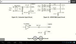
I am talking about the cs8416. See the attached grab from the datasheet.
TTL input is ok
Attachments
What is this chip?
It can play 24bit/192kHz so it can not be AK4393.
Fake AK4393, or AK4396 with wrong label?


I am talking about the cs8416. See the attached grab from the datasheet.
TTL input is ok
It is right, but only if VL (pin 21) is held at 5V; in Absolute Maximum Ratings they clearly specify: Vin MAX = VL +0.3.
In my MINI2496 board VL is held at 3.3 V.
It is right, but only if VL (pin 21) is held at 5V; in Absolute Maximum Ratings they clearly specify: Vin MAX = VL +0.3.
In my MINI2496 board VL is held at 3.3 V.
Have to agree with fulvio on this one...
I read over the CS8416 datasheet countless times, and on page 27 you'll find this;
"The input voltage range for the input multiplexer is set by the I/O power supply pin, VL. The input voltage
of the RXP[7:0] and RXN pins is also set by the level of VL. Input signals with voltage levels above VL or
below DGND may degrade performance or damage the part."
So, it would be wise to keep SPDIF input voltage below the VL. Doesn't mean it won't work, but try it at your own risk...
Or you can put a simple resistor voltage divider, but it may not be the best solution...
Or you can put a simple resistor voltage divider, but it may not be the best solution...
Thanks, I think I've fixed the problem using a compensated divider, that is a 33 pF capacitor in // with the series resistor of the divider.
In this way I can't see any difference in rise time before and after the divider.
By the way, I'm using my computer as a SPDIF source, and a 26LS32 balanced line receiver just in front of the SPDIF input of the board; in this way, without any transformer, I get more than 102 dB of S/N (20 Hz - 50 KHz band) at the audio output of the DAC board.
What do you guys think using this regulator...
http://www.diyaudio.com/forums/group-buys/206033-gb-salas-sshv2-regulator.html
hooked up like this picture? Will this have any improvements?
http://www.polkaudio.com/forums/attachment.php?attachmentid=68575&stc=1&d=1333405930
Also using a large ferrite ring in socket wiring within the case, would that help?
If you mean this one Slider.
http://www.diyaudio.com/forums/power-supplies/134801-simplistic-mosfet-hv-shunt-regs-207.html
Its a high voltage shunt and is no good for this application.
http://www.diyaudio.com/forums/power-supplies/134801-simplistic-mosfet-hv-shunt-regs-207.html
Its a high voltage shunt and is no good for this application.
volume different
Hello,
I used Dario's BOM to build this DAC. It works fine.
I notice that the analog output has a lower output (voltage) than the original DAC in the CD player. I need to add volume on the amplifier to get the level normal.
Is this normal? And how to counteract this? In other word, what parts are responsible for the amplification? I assume R23 and R29?
Haik
Have to agree with fulvio on this one...
I read over the CS8416 datasheet countless times, and on page 27 you'll find this;
"The input voltage range for the input multiplexer is set by the I/O power supply pin, VL. The input voltage
of the RXP[7:0] and RXN pins is also set by the level of VL. Input signals with voltage levels above VL or
below DGND may degrade performance or damage the part."
So, it would be wise to keep SPDIF input voltage below the VL. Doesn't mean it won't work, but try it at your own risk...
Or you can put a simple resistor voltage divider, but it may not be the best solution...
In which case, to avoid dividers and such on the spdif input, run the output of u8 to vl and all will be good.
That means the entire AK4396 (both digital and analog part) and the digital part of the CS8416 would share a common 5V supply. This can greatly affect the performance of the DAC (for the worse).
It's the lesser of two evils in which I would choose a voltage divider on SPDIF...
It's the lesser of two evils in which I would choose a voltage divider on SPDIF...
haik,
I'm using an excellent preamp with this DAC. Please check out the new thread for developments on its use an optimization. http://www.diyaudio.com/forums/analog-line-level/214380-ja-pre-myref-fe-integration.html#post3057400
I'm using an excellent preamp with this DAC. Please check out the new thread for developments on its use an optimization. http://www.diyaudio.com/forums/analog-line-level/214380-ja-pre-myref-fe-integration.html#post3057400
I really wouldn't choose either way. I was just saying it could be done that way.
Both methods are really bad. I wouldn't want to put a resistor divider on my spdif, but rf attenuators seem to be ok.
Erin, I’ve worked for about 30 years in RF and I can ensure you that a voltage divider work as well as an RF attenuator, providing you match the terminal impedances.
I would be more worried for other reasons, for example the low frequency cut of a pulse transformer, that can add a lot of intersymbol interference, that means more jitter.
How many transformers satisfy the AES/EBU requirement of a low frequency cut below 1/10 of the sampling frequency, that is below 4.4 KHz for a CD ?
Is that the reason to favor optical connection in stead of a coaxial for S/PDIF?
Fulvio, is your 26LS32 sharing the same power and ground as the AK4393 board?
What advantage do you find to using this chip?.
Erin, the power supply for 26LS32 is separate from the DAC board supply; for this one I used shunt regulators based on TL431 (see post 1871): simple, but it works.
I added to the DAC board an input selector with two optical SPDIF, two coax SPDIF and a balanced input; the last one is intended as an input for the signal coming from my computer; differential input allows ground separation and less noise from the computer PSU.
I don't like transformers (because, in my opinion, their poor response at lower frequency increase intersymbol interference), so the alternative is a balanced line receiver, like 26LS32.
Anyway, I'm going to try other line receivers, faster than 26LS32, as soon as I'll get them as free samples from TI.
- Home
- Source & Line
- Digital Line Level
- DAC 2496 (AK4393) DAC KIT With CS8416+AK4393+5532