OK it all seems good. We have lower signal on the right one, as expected from your description. Now it would be good to have some reading of the input level. It is maybe there but I doi not see it. I see visually but if you have an option of dB or V redout that would be great.
Now do all other readings as I described. It seems like youir test rig is working fine, so now we need to do all other measurements.
PS Regardles of where you are from I would not stop helping... I liked your name... I moved from Belgrade in '91.
Best
Now do all other readings as I described. It seems like youir test rig is working fine, so now we need to do all other measurements.
PS Regardles of where you are from I would not stop helping... I liked your name... I moved from Belgrade in '91.
Best
OK, I hope I made it all good.
First, left and right INPUT channels do not have same specifications, so I repeated and continued measurements on the LEFT input (so images on previous page do not relate to these images here).
Im not sure how to measure Input Level. There is some Input Level on the screenshots, but Im not sure if that is it. Measuring with Voltmeter on the connectors, all are around 0mV except the problematic one that is about 23mV.
The only think I couldn't measure is with half-way pulled connector.
What now, please?
1 Unproblematic channel
2 Problematic channel
3 Unproblematic channel with T and S soldered with wire
4 Problematic channel with T and S soldered
5 Unproblematic channel with R and S soldered
6 Problematic with R and S soldered
I liked that name. It sounds very powerful when accented on the first A, jugoslAvija. It could be understand like something like some "institution" slAvia of the people of South Slavians. Like "This here is Jugo Slavija". full stop. If jugoslavija succeeded to exist it would be the biggest success of all south slavians! bla bla but thats true")
Anyway i like photography, and I see very nice photographs and really unique images on the site in your sig. Thanks for sharing and letting us enjoy viewing. Keep up!
First, left and right INPUT channels do not have same specifications, so I repeated and continued measurements on the LEFT input (so images on previous page do not relate to these images here).
Im not sure how to measure Input Level. There is some Input Level on the screenshots, but Im not sure if that is it. Measuring with Voltmeter on the connectors, all are around 0mV except the problematic one that is about 23mV.
The only think I couldn't measure is with half-way pulled connector.
What now, please?
1 Unproblematic channel
An externally hosted image should be here but it was not working when we last tested it.
2 Problematic channel
An externally hosted image should be here but it was not working when we last tested it.
3 Unproblematic channel with T and S soldered with wire
An externally hosted image should be here but it was not working when we last tested it.
4 Problematic channel with T and S soldered
An externally hosted image should be here but it was not working when we last tested it.
5 Unproblematic channel with R and S soldered
An externally hosted image should be here but it was not working when we last tested it.
6 Problematic with R and S soldered
An externally hosted image should be here but it was not working when we last tested it.
I liked that name. It sounds very powerful when accented on the first A, jugoslAvija. It could be understand like something like some "institution" slAvia of the people of South Slavians. Like "This here is Jugo Slavija". full stop. If jugoslavija succeeded to exist it would be the biggest success of all south slavians! bla bla but thats true
Anyway i like photography, and I see very nice photographs and really unique images on the site in your sig. Thanks for sharing and letting us enjoy viewing. Keep up!
Last edited by a moderator:
Hello,
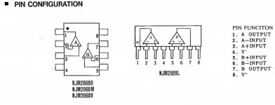
now if you are positive that image 4 is R and S connected, than positive side of your balanced signal has a problem. The only problem now is that any further work will require some better test equipment and some surgical skills. If you look at the circuit picture you posted, you will see two opamps JRC 2068 and four SMD transistors. What you would need to do is to trace backward path from connector for that problematic positive side of the signal. The best way of doing it is if you have the very same sine signal going on and than by using scope probe observe at what point you are loosing the full signal. The way how to do that in such a tight environment, is to attach small wires that you could hook your scope probe to. Without having schematic, my guess is that opamps are used to buffer/amplify signal and transistors are used for mute function. Obviously I could be very wrong since I have no knowledge of the circuit, but just my guess. At least the first thing you would need to do is to download data sheet for transistor and opamp.
I have to warn you that really without proper equipment any further work is almost impossible for you. Even if you find out what is the source of a problem, than you will need an smd workstation (hot air) to unsolder this opamp an example, without loosing any resistors or caps around it.
Maybe is better to take this to someone else who does have a appropriate equipment and ask for help. That way you will see how it is done and have your problem solved.
Best of luck
Last edited:
Thanks alot for helping, AR2! Really nice from you.
Anyway, I had plans for modding the card, by replacing OPAMPs for some better and maybe CAPs.
So, You believe the problem could be OPAMP or SMD. I have a friend with hot air, for start, I could try swapping L with R OPAMP to see if the problem would shift to the other channel. If so, I could order new OPAMPS. I believe same relates to the SMDs. I simply dont believe I could find a service that could easily fix the problem, in my small city. There are services with scopes, but I'm afraid about just explaining them the problem... The question is, is there any other component that could make this kind of problem, like CAP, resistor or what else? My card has MANY working hours!
Thanks, will let You know if opamps and smd swapping shifted the problem to the other channel.
Hold your horses!
I do not think it is a good idea to do what you are attempting to do since in the process you could burn both devices. First - terminology. Both parts, and all other parts on your board are SMD - Surface Mount Devices. So what we are talking are ether opamp or transistor. This is what I am guessing just by looking at your board. The reason I am saying to use scope is to find out exactly where the signal shifts. What if the problem is at the DAC, what is quite possible. It is my optimistic assumption that they do not have any cap in the path of the signal, just by looking at the board. SMD caps that we see around the opamp should be bypass caps, and since we are having a problem only with one side, or 1/2 of the signal coming from one opamp, I do not think the problem is with that. Again just my guess.
Only with the scope you will be able to look and follow signal and find out where is that signal changes. If you have all signals as they should be at the input at the opamp, and difference between outputs than you know where the problem is. If by any chance you have a difference in signal at the input of the opamp, than you know that on the way from DAC you have a problem.
If you have a decent multimeter you could even use that to measure, but do not go higher in frequency than 1KHz as many multimeters are not that good at higher frequencies (good ones could be good up to 100 KHz) Again, if you do not use small wires and you attempt to touch legs directly with probes you will have a great chance of shortening something that could do bigger damage.
Another option is that you could make your own probe and wire those as input to the card so that you could use your software to act as scope. Obviously this is even more trickier and you have to be very careful. Your best and safest bet is to solder wires and than turn on computer instead of trying to do it by touching.
Keep us posted
OK, just to check if I got it right:
1. make a TS connector with 2 wires (wires should be like probes), connect to the input of a sound card. scope software I already have
2. solder 2 thin wires to the signal path: opamp inputs, outputs etc , connect them to the "probes" and measure result of 1khz sine tone on the scope. repeat procedure for every half of the signal (L+, L-, R+, R-)
Ill start measuring at the opamps, but only Im not sure what pins should I measure. I know they are dual opamps, but If I want to measure inputs, should I measure between +Input and -Input? There are: Output, +Input, -Input and V pins on every side of opamp. And if I want to measure the outputs of the opamp, what should I measure between: output and ground anywhere on the card or between output and V?
If I got it right, it seems fairly doable for me, except very, very small components on that analog board. They are so tiny!
Attachments
You could make cable with two wires and two connectors - one on each side. Plug them like a loop, one on input and one on output of the channel you are testing. On the output side, short circuit SLEVE and RING. Make wire that should go to the TIP much longer, and use that to connect to the tin wire that will be soldered to the testing points. That means that your TIP on the output connector is not connected.
Solder really thin wire, something like 30 - 32 gage solid wire to the opamp output pins and those are pins 1 and 7. You could do the same for the inputs, pins 2 and 3 and 5 and 6. Do not connect anything to pins 4 and 8 those are your positive and negative voltages. That is why you have to be very careful when you are wiring not to short circuit to those pins because that way you could burn your input (if there is no cap at the input to block DC)
Wire that you could use for soldering - phone wire, obviously just a single strand. That is very handy to have for many other purposes. That is thicker than what I suggested above, but I doubt you will be able to find Kynar wire, something like this
Amazon.com: OK Ind Wire Roll, Insulated Kynar, 30 AWG, 100' Roll, Blue: Home Improvement
So my point is, you will be measuring, just like in the first test, voltages between GROUND and POSITIVE or NEGATIVE side of the signal. Do it for opamp and than do check transistor. You have to find out what is the transistor used and than download the data sheet to find out what is what.
When you work on this, use the biggest loop you could find. Something like 10X will work really well. Get the thinnest solder you could find. Also have ready fine braided wire. If you create bridge between pins, no worries, just use braided wire to clean it up. Take your time and do it slowly with enough light and with strong loop. This is not too bad, those pins are not that close like some more complex ICs. You could do it.
Best
Vladimir
Hello,
This is what I did:
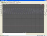
made a cable with 2 TRS connectors; wired R+S on one (output) connector with wire to a S on input connector; T from input connector wire, jumping to pins 1 and 7 on output opamps. During the measurement I did not replace the input/output channels: all was setup, the only thing that I moved between measurements is the 1 probe wire (between opamp pins). I am not sure if this is ok? Anyway, the results are exactly the same on both output opamps on both pins (1 and 7). All 4 screenshots are the same.
If the measurement is ok I would say the DAC and output opamps are ok?
This is what I did:
made a cable with 2 TRS connectors; wired R+S on one (output) connector with wire to a S on input connector; T from input connector wire, jumping to pins 1 and 7 on output opamps. During the measurement I did not replace the input/output channels: all was setup, the only thing that I moved between measurements is the 1 probe wire (between opamp pins). I am not sure if this is ok? Anyway, the results are exactly the same on both output opamps on both pins (1 and 7). All 4 screenshots are the same.
If the measurement is ok I would say the DAC and output opamps are ok?
Attachments

Last edited:
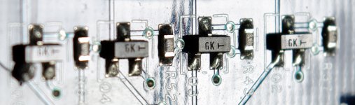
All that is written on top of transistors is "GK" with one letter "T" but "T" is rotated for 90degrees, so it looks like "GK |-"
Here, I found something similar: the dimensions of transistor are approx the same, but the pins are B, C and E, which I dont understand: DDTC114GKA-7 datasheet, DDTC114GKA-7 ?????, DDTC114GKA-7 ?????, pdf datenblatt - Diodes Incorporated - NPN PRE-BIASED SMALL SIGNAL SC-59 SURFACE MOUNT TRANSISTOR ::: ALLDATASHEET :::
I see which of the 3 pins goes to the connectors pin, so I can measure there, but, if I got it right, I should get same results like measuring on the connector?
Last edited:
B- Base E - emitter C - collector
No we cannot go like that on transistors, by size and look.
Good, you see there was no need to move around opamps. Now since we know that opamps are OK there are only two variables - transistors and connectors. Now I woud do the same test but behind transistors. Find where signal leads toward output connector and measure there. That will be AFTER transistors. Same test same cable, just different location.
OK, measured all 4 transistors. 1st gives bad results, 2nd gives no result (because it is connected to ground on the connector I made), 3rd gives ok result, 4th ok.
Thats it?
Now what? I need new transistor! Ok, but what exactly to look for?!
1st, 3rd and 4th (from bottom to top on the posted picture od board) transistor result in attachment.
Thats it?
Now what? I need new transistor! Ok, but what exactly to look for?!
1st, 3rd and 4th (from bottom to top on the posted picture od board) transistor result in attachment.
Attachments


Last edited:
OK, measured all 4 transistors. 1st gives bad results, 2nd gives no result (because it is connected to ground on the connector I made), 3rd gives ok result, 4th ok.
Thats it?
Now what? I need new transistor! Ok, but what exactly to look for?!
1st, 3rd and 4th (from bottom to top on the posted picture od board) transistor result in attachment.
OK, congratulation. You did very fine job and you find out what is the problem. Now, that transistor has to have some markings. We ether need schematics or you have to carefully inspect with loop to find out what is written on it.
I also invite anyone else who might know something more about this card to pitch in. Certainly schematic would be greatly appreciated. If not that, than anyone has any suggestion what to do at this point? I have no idea what is the transistor, is it jFet, Mosfet or bipolar? Any other ideas would be great. Jugoslavija, seat tight, I am sure we will be able to find some solution.
Thanks
Vladimir
try to inspect are those transistors mute ones ;
you can check that - is any of pins ( on all 4 ) connected to gnd ?
in that case - if another pin ( of all 4 ) is connected to output , they certainly are mute transistors
in that case - just cut trace going from that suspicious one to signal , then try quality of signal
you can check that - is any of pins ( on all 4 ) connected to gnd ?
in that case - if another pin ( of all 4 ) is connected to output , they certainly are mute transistors
in that case - just cut trace going from that suspicious one to signal , then try quality of signal
Hi, thanks for helping;
So, we have:
All 4 transistors have one output pin - thats the one I measured on (left pin on the side where there are 2 pins). One of the other pins should be input, right? And the third could be GND? So, I should check other 2 pins if one of them is GND? I do that by measuring the Voltage between that 2 pins and metal chasis of the card, looking for 0V, and that should be GND? Or turn off the card and measure resistance between pins and chassis, again looking for 0 ohms?
Zen Mod, you are from Serbia, is it possible to find those transistors new, to buy, here?
Hello,
I measured: one probe connected to output SLEEVE, and other probe connected to pins;
On pin 1 (the one I measured transistors above) resistance is about 46ohm, on pin 2 is 0.8 ohm and on pin 3 is 1.
Pin 2 should be gnd, right? Multimeter is not 'TOPL' and if i connect probes directly result is also 0.8ohms.
These measurements results are equal for all 4 transistors.
Last edited:
- Status
- This old topic is closed. If you want to reopen this topic, contact a moderator using the "Report Post" button.
- Home
- Source & Line
- Digital Line Level
- Emu 1212m problems