[snip]Its not a shunt type regulator and dont have cap. multiplication, look carefully.
Advantages of this schematic is
-no electrolitycs and it problems
-low and stable(resistive) output impedance
-Perfect transient response (Series regulator(317\337) is completely detached from load)
-High ripple rejection and low noise
-No dependence noise-output current, output impedance-output current
-no global nfb
Disadvantages
-Efficiency
Ohm's law R=U\I ... 17ohms
So, Nazar, I still don't get it. The shunt (it is a shunt, no doubt) pulls a constant current from the regulator, the same current a 17 ohms resistor would pull.
All these advantages you list are the result of a resistor load on the regulator?
The shunt (transistor or resistor) does nothing to the Zout, the Zout is the Zout of the 317, (which is something in the order of 0.02 ohms up till 10kHz when it starts to rise), in parallel with 17 ohms and the B-E junction. It still rises with frequency, therefore is still inductive.
Can you please explain?
When you change the load current from, say, 50mA to 100mA, how much does the final output voltage change? That is the indication for the Zout.
I expect it to be very much larger than 1 ohms, but I may be wrong.
jd
Last edited:
But the load regulation is not as good as with NFB ?
I did a simulation of the discrete part,
with ideal supply and reference instead of LM317.
Simulated load was active sine source with expected Ri and 1 Vpp.
Bernhard, what did you see in the sim?
jd
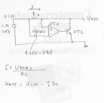
AFAIK the simplified diagram of the circuit is as follow
VT1 is represented as an (ideal: infinite gain, bandwidth, ...) OP Amp
VBias = 1.25 - Vbe
where
1.25 = Vref of LM317
Vbe = Vbe of VT1
So we get that the current flowing in R2 is constant and his value is:
Ir2 = VBias / R2
Vout = Vin - Ir2 * R2 which is constant (regardless the current flowing in the output load)
The output resistance is 0 (zero) due to the fact that current and voltage are constant
We observe that:
- The current supplied by the LM317 is constant regardless the load current
- VT2 try to sink the current not flowing into the load
If we take into account the finite gain of VT1 (non ideal Op Amp) we guess that output resistence of the circuit is
Rout = R2 / AVvt1
where AVvt1 is the (finite and frequency dependent) gain of VT1
We must also take into account the Vbe modulation of VT1 due to the change of the emitter current of VT1
A simulation is in order")
VT1 is represented as an (ideal: infinite gain, bandwidth, ...) OP Amp
VBias = 1.25 - Vbe
where
1.25 = Vref of LM317
Vbe = Vbe of VT1
So we get that the current flowing in R2 is constant and his value is:
Ir2 = VBias / R2
Vout = Vin - Ir2 * R2 which is constant (regardless the current flowing in the output load)
The output resistance is 0 (zero) due to the fact that current and voltage are constant
We observe that:
- The current supplied by the LM317 is constant regardless the load current
- VT2 try to sink the current not flowing into the load
If we take into account the finite gain of VT1 (non ideal Op Amp) we guess that output resistence of the circuit is
Rout = R2 / AVvt1
where AVvt1 is the (finite and frequency dependent) gain of VT1
We must also take into account the Vbe modulation of VT1 due to the change of the emitter current of VT1
A simulation is in order
Attachments
Last edited:
AFAIK the simplified diagram of the circuit is as follow
VT1 is represented as an (ideal: infinite gain, bandwidth, ...) OP Amp
VBias = 1.25 - Vbe
where
1.25 = Vref of LM317
Vbe = Vbe of VT1
So we get that the current flowing in R2 is constant and his value is:
Ir2 = VBias / R2
Vout = Vin - Ir2 * R2 which is constant (regardless the current flowing in the output load)
The output resistance is 0 (zero) due to the fact that current and voltage are constant
We observe that:
- The current supplied by the LM317 is constant regardless the load current
- VT2 try to sink the current not flowing into the load
If we take into account the finite gain of VT1 (non ideal Op Amp) we guess that output resistence of the circuit is
Rout = R2 / AVvt1
where AVvt1 is the (finite and frequency dependent) gain of Vt1
We must also take into account the Vbe modulation of Vt1 due to the change of the emitter current of VT1
A simulation is in order
I think your analysis is right on target. This is what shunts do: absorb the variations in load current, thereby presenting a constant voltage to the load looking as if it comes from a very low (ideally zero) Zout. As you noted, the limit on reaching zero Zout is the 'loop gain' of the shunt.
But it can only work within the range of the shunt current which must be low for the type of transistor used. Do we know the actual value of R2? I thought about 17 ohms for a 35mA shunt current but I think Nasar indicated a lower dissipation in the shunt so consequently a lower shunt current and a higher R2 value.
jd
diy_audio_fo good, but VT1 and VT2 together forms superbeta transistor.
Practical use DAC Picardian chord v1.2

NazarNasar
Practical use DAC Picardian chord v1.2
diy_audio_fo good, but VT1 and VT2 together forms superbeta transistor.
Nazar
Practical use DAC Picardian chord v1.2
Nazar,
Is there a point to this post or is it only used to advertise your stuff?
jd
Hi, yes, on HFIs the purpose of the no. of 0.1 caps at the output to reduce
impedance
all caps as close as possibleis the last cap place close to the pins of the IC
Is there a point to this post or is it only used to advertise your stuff?
Do we know the actual value of R2? I...
If there is no need i delete my previous post
Last edited:
Hi Nazar,
I'm building your PSU for my RIAA phono (LME49990 in, passive RIAA, LME49713 out). I have 100n from the schematic (output caps) very close to my
power in pins on the 49713 but not as close for the 49990.
I was wondering, do I still need local bypass caps? I was thinking of 4.7uF MKP parallel to 100n NPO, from each rail to GND.
Thank you
SUPPLY BYPASSING
To achieve a low noise and high-speed audio performance, power supply bypassing is extremely important.
Applying multiple bypass capacitors is highly recommended. From experiment results, a 10μF tantalum, 2.2μF
ceramic, and a 0.47μF ceramic work well. All bypass capacitors leads should be very short. The ground leads of
capacitors should also be separated to reduce the inductance to ground. To obtain the best result, a large
ground plane layout technique is recommended and it was applied in the LME49990 evaluation board.
Most op-amp manufacturers produce a guideline and app notes for decoupling, use engineering not your ears (they tell you nothing about decoupling), this is more critical these days because of the amount of RF and other high frequency noise present in the envoironment.
our ears perfectly hear result of good decoupling etcuse engineering not your ears
(and of good PCB tracing, low EMI, etc etc etc)- Status
- This old topic is closed. If you want to reopen this topic, contact a moderator using the "Report Post" button.
- Home
- Source & Line
- Digital Line Level
- Capacitorless PSU