PS. If you buy that box and rip it apart, you can make your remote controlled relay replace the switch on the box rather than switching the USB lines themselves
That's very true. But I'm trying to understand - I'm all for doing it properly, but in what way does this differ from the way a relay would switch the wires? You've got me searching for USB switching ICs - one of the first I found is this one. The schematic shows that the main function is just to switch over the data lines - it doesn't even bother with the power lines. It has various protection features, presumably to cope with whatever it gets connected to, but is any of that necessary for a device that would sit permanently between a DAC (DLCP) and a couple of computers (RPi and external PC)?
For my own PCB my wires would not be centimetres apart. They'd attach to the board via ribbon cable plugs to 0.1" pin headers, and the traces on the PCB could be the absolute minimum PCB distance apart (certainly no further apart than they would be to use one of these ICs). I'd see to it that the line lengths would be identical throughout.
Electronic design considerations discussed here. The article may be from 2000, but the considerations haven't changed
At 480 Mbits/s, Signal Integrity Becomes An Issue In USB 2.0 Designs | Electronic Design
USB 2.0 High Speed runs at 480Mbps, so your signals contain a higher bandwidth than this. Not really the sort of thing to switch through a standard relay - ie. you're lucky it's working at all.
Nor the sort of thing to introduce an aerial for, which is what all your circuitry is effectively doing
As Julf said
And yes - there are always problems related to running/connecting multiple earth points together.
Now, switching your USB power by relay, no high bandwidth signalling concerns there.
But does the DLCP actually need power on the USB?
At 480 Mbits/s, Signal Integrity Becomes An Issue In USB 2.0 Designs | Electronic Design
USB 2.0 High Speed runs at 480Mbps, so your signals contain a higher bandwidth than this. Not really the sort of thing to switch through a standard relay - ie. you're lucky it's working at all.
Nor the sort of thing to introduce an aerial for, which is what all your circuitry is effectively doing
As Julf said
Shows how robustly specified USB is.")
And yes - there are always problems related to running/connecting multiple earth points together.
Now, switching your USB power by relay, no high bandwidth signalling concerns there.
But does the DLCP actually need power on the USB?
I'm not buying it.
Switching all four wires simultaneously, via relays, is surely the mechanical and functional equivalent of pulling out one cable and inserting the other. Apart from speed, obviously.
And I can't see how the potential for this PCB to act as an aerial differs from the use of an IC on a PCB (e.g. on an external switcher box, or even a hub, any of which will route the wires from the sockets via traces on the PCB).
That's a shame
Please do read and understand the linked article,
and search for others so you understand high speed signal design & layout:
^^ this is important to USB 2 implementation, but you seem to imply it should all be ignored and any circuit design will be fine.
You aren't proposing the equivalent of uplugging a cable (screened, shielded, balanced) and plugging in another; you're proposing the equivalent of removing all the screening from a large length of USB cable and splaying out all the wires. There is a world of difference between detailed board layout of traces to maintain/minimise high-speed signal integrity and switching it through a common or garden relay.
This really is a case of trying to understand what should be going on with these signals at hf, and that if your current relay solution works, then it's by good fortune.
Please do read and understand the linked article,
and search for others so you understand high speed signal design & layout:
"In addition, electromagnetic interference (EMI) at edge rates of 12 Mbits/s isn't particularly troublesome. But, current board-layout implementations that were convenient for USB 1.0 components may require significant redesign for USB 2.0 components. New board-routing guidelines require closer attention to attenuation, jitter budgets, package/board/chassis design, and EMI/EMC shielding."
"Consider, for example, that the better-performing devices won't put high-speed pins in the corners of the package, because wirebonds are the longest in the corners. Instead, high-speed pins should be placed in the middle of one of the sides of the package where the wirebond length will be the shortest. The board designer must keep trace lengths to a minimum. Therefore, when selecting a multiport design, the best choice might be a chip where all high-speed ports are on the same side of the package. If high-speed ports are laid out one per side, then the board designer may be unpleasantly surprised as traces are laid down."
"In the design of a board containing USB 2.0 functionality, the number of layers, power and ground placement, and connector placement have become significantly more critical."
"Match Trace Impedances"
"Running signals through vias creates an impedance change that can be significant. Even 90° corners will create problems."
etc.."Consider, for example, that the better-performing devices won't put high-speed pins in the corners of the package, because wirebonds are the longest in the corners. Instead, high-speed pins should be placed in the middle of one of the sides of the package where the wirebond length will be the shortest. The board designer must keep trace lengths to a minimum. Therefore, when selecting a multiport design, the best choice might be a chip where all high-speed ports are on the same side of the package. If high-speed ports are laid out one per side, then the board designer may be unpleasantly surprised as traces are laid down."
"In the design of a board containing USB 2.0 functionality, the number of layers, power and ground placement, and connector placement have become significantly more critical."
"Match Trace Impedances"
"Running signals through vias creates an impedance change that can be significant. Even 90° corners will create problems."
^^ this is important to USB 2 implementation, but you seem to imply it should all be ignored and any circuit design will be fine.
You aren't proposing the equivalent of uplugging a cable (screened, shielded, balanced) and plugging in another; you're proposing the equivalent of removing all the screening from a large length of USB cable and splaying out all the wires. There is a world of difference between detailed board layout of traces to maintain/minimise high-speed signal integrity and switching it through a common or garden relay.
This really is a case of trying to understand what should be going on with these signals at hf, and that if your current relay solution works, then it's by good fortune.
Please do read and understand the linked article,
and search for others so you understand high speed signal design & layout:
I'm looking forward to having a read through that this evening. It looks like a useful article, thank you. HF signals are way beyond my comfort zone, but if there are some useful guidelines, such as the ones you highlighted, I'm all ears.
This is the sort of thing I had in mind.

The D+ and D- lines are equal lengths, and I've avoided any sharp corners. The power lines don't need this consideration, so they go through their own relay, with some unequal lengths and the traditional 45 degree bends.
All the traces are on one layer - not sure whether that's good or bad yet - need to do more reading.
I think I may have put the relay outlines in the wrong way round, but that's easily fixed. I'll need to redo it, because the USB wires in the DLCP are arranged D+, D-, Vcc, GND. If anything, that will make the layout easier I think.
Had a bit more of a play with a relay board design. The relay that will switch the Vcc and GND lines has been swapped over to match the order of the lines on the DLCP ribbon cable, and I've tweaked the routing of the D+ and D- lines and added a ground plane. Still reading up on the subject, and finding my way around 'Eagle' for designing PCBs. Not sure if I should put more effort into routing the data lines over the ground plane, but that's not easy without running them closer to the Vcc and GND lines - not sure what the priority is.
In the meantime my RPi button board PCBs arrived early, so I built one up to mirror the DLCP control panel. My first PCB, and it worked first time! Not sure I'll keep the black button caps on - I have some orange ones that might replace some of them, and they'd be a good match for the Hypex logo that I'm considering incorporating into the faceplate somehow.
An externally hosted image should be here but it was not working when we last tested it.
An externally hosted image should be here but it was not working when we last tested it.
Last edited:
That's a neat idea. In previous amplifier builds I simply mounted separate chassis-mount Neutrik-style sockets with separately soldered cables, and would have done the same again with my DLCP integrated amp build had you not posted this. I may do something similar now though. As an integrated amp, all I really need is some 'Speakon' connectors for the 6 speaker channels - in my previous 4-channel power amp I used a couple of 4-pole connectors but for this 6-channel build I will probably use 6 separate 2-pole connectors.
So my rear panel is going to get a bit crowded, with the long DLCP input board and 6 Speakon connectors. And I'd rather like to route the DLCP outputs and UcD inputs to the back panel as well, so that the amp can be used as a DSP pre-amp or a 6-channel power amp, as well as an integrated amp. The idea would be to provide external links between the DLCP outputs and the UcD inputs. My old NAD 3020A has rigid U-links in the single-ended sockets on the back panel, and I envisage something similar, but using balanced connections. But 6 balanced outputs AND 6 balanced inputs would make the back panel very crowded indeed if using full-sized XLR sockets.
So my question for the experts here is what connection types to use to keep the back panel real estate to a minimum. I've seen mini XLR sockets, but I wonder now if I could use the same 4-way Molex Microfit connectors that are used on the DLCP (and Neheb's output board). I could use Molex-to-Molex U-links when the amp is being used as an integrated amp, and I could make Molex-to-XLR adapters to use either half of the amp on its own. Are they suitable for chassis mounting?
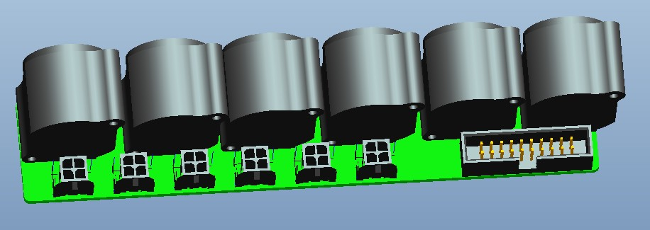
Those Molex connectors come in horizontal PCB-mount packages as well as the vertical mount packages used on the DLCP and Neheb's board, so I think they could be used for my DLCP-to-power-amp links on the rear panel. I've drawn up a PCB that has two rows of 6 - one row for the outward-facing sockets on the rear panel, and one as inward-facing sockets so that the DLCP can connect to the rear panel with the mating plugs. I'd use two of these boards - one for DLCP outputs and one for the power amp inputs.
To make it completely flexible I've also drawn up an adapter board for my UcD400 OEM modules to include the same Molex socket. It's a shameless copy (from photos I found online) of the 'official' Hypex OEM adapter, which you can't buy unless you're an OEM, but with the 4-pin header changed to the Molex socket.
So with this I could connect the DLCP directly to each UcD module, or I could go via the link boards on the rear panel.
An externally hosted image should be here but it was not working when we last tested it.
An externally hosted image should be here but it was not working when we last tested it.
I could do with some advice regarding current flows within the power supply lines and the speaker outputs in a UcD400, to check the trace widths for those terminals. In my first draft of my adapter board above I sized those traces to look about the same as the ones used on the official Hypex board, but of course I can't tell how thick their copper layers are from photos.
The SMPS1200A400 provides 2x63Vdc, and the UcD400 is rated as 400W into 4 Ohms and 250W into 8 Ohms. So if driven to these power levels, how much current would flow down each power supply trace, and how much could travel along the LS+ trace? Am I right that each side of the power supply will be responsible for half the power (which is the same as saying that the potential difference between the rails is 2x63Vdc)? So each rail would need to carry 200(W)/63(V) = 3.2A. I'll be powering 8 Ohm speakers, and I know that I'll never use all that power, but I don't want the capability to be limited by a blunder on my part.
And what about the speaker terminal? How do I quantify current flow in that trace? The UcD400 gives a voltage gain of 26.5dB, and the DLCP outputs 2.59V, so I *think* that means the output voltage could be up to 55V. What next? 400W/55V = 7.3A ??? I'm sure there's more to it than that - what about 'rms' for instance?
I've had a go at adjusting the layout and beefing up the traces, because it's cheaper to do that with 1oz copper than to go for 2oz copper and narrower traces. According to this calculator my new traces should cope with any of the numbers I've derived above.
But are my derivations anywhere near correct?
An externally hosted image should be here but it was not working when we last tested it.
Last edited:
And what about the speaker terminal? How do I quantify current flow in that trace? The UcD400 gives a voltage gain of 26.5dB, and the DLCP outputs 2.59V, so I *think* that means the output voltage could be up to 55V. What next? 400W/55V = 7.3A ??? I'm sure there's more to it than that - what about 'rms' for instance?
The amp will definitely output more than 400 W during transients - to be safe, you could use the 20 A current limit as the maximum current.
Yikes - that means roughly twice as wide as the trace in my revised design, *and* 2oz copper. There isn't room for twice the width (it's somewhat limited by the area of the 5 pins used for this signal), so I'll put a trace on the other layer as well - there's more than enough ground plane on the other layer to lose some to that extra trace.
Yikes - that means roughly twice as wide as the trace in my revised design, *and* 2oz copper. There isn't room for twice the width (it's somewhat limited by the area of the 5 pins used for this signal), so I'll put a trace on the other layer as well - there's more than enough ground plane on the other layer to lose some to that extra trace.
The 20 A current will of course only be for very short peaks, average current will be much lower.
The 20 A current will of course only be for very short peaks, average current will be much lower.
That calculator I linked to above allows for a permissible temperature rise to be factored in. I think that briefly exceeding a limit defined by, say, 10A + 10 degree C temperature rise, would not instantly burn out the track, it would just heat it up a bit. So I think a more pragmatic approach will suffice. Maybe I can get away with the cheaper 1oz copper after all, if I put a matching track on the same side as the ground plane.
That calculator I linked to above allows for a permissible temperature rise to be factored in. I think that briefly exceeding a limit defined by, say, 10A + 10 degree C temperature rise, would not instantly burn out the track, it would just heat it up a bit. So I think a more pragmatic approach will suffice. Maybe I can get away with the cheaper 1oz copper after all, if I put a matching track on the same side as the ground plane.
Yes, you'll probably be fine.
I've added traces to the side of the board carrying the ground plane. I reorganised the layout again so that the ground plane was not compromised by these extra traces (the route back from the LS- terminal has to be as good as the route to the LS+ terminal).
I reckon these traces will handle 10A continuously and only warm up a few degrees, and even at 20A continuous they wouldn't be uncomfortably hot.
I also adjusted the hole positions so that they'll hopefully align with the pre-drilled grid of holes in the baseplate of the Dissipante enclosure that I'm planning to use. Unlike the official OEM adapter that mounts in the same plane as the UcD400 I'm intending that my boards will sit at right angles to the UcD, so I'm intending that the adapters will bolt to the baseplate and leave the amplifier modules standing with their backing plates nicely touching the heatsink sides of the enclosure. That's the plan anyway!
An externally hosted image should be here but it was not working when we last tested it.
An externally hosted image should be here but it was not working when we last tested it.
In my adapter board I had blindly copied the 10-pin connector that is on the official OEM adaptor, but there's a note in the documentation for the official adapter that says:
"Caution: This connector is not compatible with our range of power supplies. Connecting this connector to a Hypex SMPS will damage your power supply!".
I'll be using an SMPS1200A400 for my 6 UcD400OEMs. So I'm wondering now which pins I really need from that connector. Can someone with knowledge of these UcD components help me to understand their roles?
J1.1: GND
J1.2: GND
J1.3: NC
J1.4: Current Limiting Monitoring (Output)
J1.5: Amplifier Ready (Output)
J1.6: ON/OFF control
J1.7: Buffered Non-Inverting Audio Input
J1.8: Buffered Inverting Audio Input
J1.9: Clipping Detection (Output)
J1.10: DC-Error (Output)
The two audio inputs (J1.7 and J1.8) are on my Molex connector, so not needed.
The ON/OFF control (J1.6) is also on my Molex connector, but this would give the DLCP control over the amplifier (since the Molex connects to the matching Molex sockets (J10 to J15) on the DLCP). In this configuration I believe the amplifier could potentially come on before the SMPS is ready, resulting in a pop. I believe it may be more appropriate to let the SMPS control the amplifier ON/OFF state, so that the amplifier only comes on when the SMPS is ready for it. This might be a better guarantee of pop-free start-up. Is that correct? If so, I might put a jumper on the adapter board so that I can select between SMPS ON/OFF control and DLCP ON/OFF control.
The DC-Error output should go back to the SMPS, so it shuts down in the event of an error. I think this output from each of my amplifier channels can go back to the common input on the SMPS, so that a fault in any one of them shuts down the SMPS - is that correct?
So other than GND and NC, that leaves:
J1.4: Current Limiting Monitoring (Output)
J1.5: Amplifier Ready (Output)
J1.9: Clipping Detection (Output)
Am I right that these last three don't have a simple connection anywhere on the DLCP or SMPS? What is their purpose? Are they just there to drive LEDs for instance, to give a visual warning of these conditions? Or could they be used to control the SMPS or DLCP somehow?
If they don't have a built-in role, I may change my board layout (again) to replace the 10-pin header with a 5-pin header to carry these three pins (in case I need them in future) plus the DC-Error output and the SMPS ON/OFF output, and add a jumper to select which ON/OFF signal to obey.
Does all of that make sense?
Question on the plate amplifier loudspeaker connections.
The FA plates are supplied with a loudspeaker connection cord (125 cm if I remember correctly, some gauge I can't remember).
- Should I use this (it might be part of the transfer function with it's resistance) or can I use my existing cable (very stiff 3-4 mm2 cable)?
Just my tinkering.
The FA plates are supplied with a loudspeaker connection cord (125 cm if I remember correctly, some gauge I can't remember).
- Should I use this (it might be part of the transfer function with it's resistance) or can I use my existing cable (very stiff 3-4 mm2 cable)?
Just my tinkering.
- Home
- Source & Line
- Digital Line Level
- Hypex DSP module(s)