Please look at this datasheet of DAC8811 - http://focus.ti.com/lit/ds/symlink/dac8811.pdf
What exactly is the purpose of pin Rfb ? I know its something to do with feedback but I am not quite clear. Does this have to be connected ? What would happen if its not used ?
Please advise.
Thanks.
What exactly is the purpose of pin Rfb ? I know its something to do with feedback but I am not quite clear. Does this have to be connected ? What would happen if its not used ?
Please advise.
Thanks.
Please look at this datasheet of DAC8811 - http://focus.ti.com/lit/ds/symlink/dac8811.pdf
What exactly is the purpose of pin Rfb ? I know its something to do with feedback but I am not quite clear. Does this have to be connected ? What would happen if its not used ?
Please advise.
Thanks.
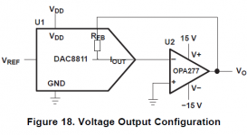
The output of the DAC is a current, not a voltage. The output amplifier in figure 18 on page 8 converts the current to a voltage. Rfb can be anything you want but the manufacturer provides a trimmed one in the DAC chip so you can achieve the published specs. You're free to substitute your own value if it suits you better but be aware that there are always trade-offs when you make changes.
G²
I guess I understand the purpose of the resistor 'rfb' inside the chip but I am not able to understand its usage for the purpose of "feedback". What if there was no opamp i-v conversion stage ?
Maybe lets try by example -
Explain to me how and why would you connect the Rfb pin to, if you were to use a simple resistor I-V conversion stage ? I believe the I-V conversion resistor would go between Iout and Gnd ?
Maybe lets try by example -
Explain to me how and why would you connect the Rfb pin to, if you were to use a simple resistor I-V conversion stage ? I believe the I-V conversion resistor would go between Iout and Gnd ?
Rfb is the I-V conversion resistor. You have the possibility to use it or not.
Either directly to the ground (like you want, but not what TI wants) or better in an OpAmp loop to provide a virtual zero impedance to ground at the DAC output like it is shown by manufacturer.
Either directly to the ground (like you want, but not what TI wants) or better in an OpAmp loop to provide a virtual zero impedance to ground at the DAC output like it is shown by manufacturer.
Attachments
Last edited:
The primary merit of putting a resistor in recommended feedback path of an opamp is this : bandwidth.
Imagine simply putting a resistor from IOUT to GND. There will be a capacitance on that node to GND also ... pin capacitance on the DAC itself, trace capacitance associated with the resistor itself, plus the input capacitance of whatever is "observing" the output voltage. That total "parasitic" capacitance, in conjunction with the resistance of the I/V resistor, will determine the bandwidth of the I/V conversion ... since the I/V resistor is the resistance "seen" by the capacitance.
Now let's examine the opamp configuration. Any parasitic capacitance on the IOUT pin will no longer matter ... since the opamp holds that pin to a virtual ground. And, any parasitic capacitance on the opamp output will "see" the closed-loop output impedance of the opamp, rather than the RFB resistance.
There are other motivations to use the opamp as well ... there will be a "voltage compliance" on the DAC output pin, that limits how high/low the voltage can move. The current source output will not be "ideal" either, meaning the output current will be a tiny function of output voltage ... which may limit ultimate accuracy. These factors are non-issues if the DAC drives the current into a virtual ground.
YES ... it's wise to use the recommended opamp configuration, with the I/V resistor in the feedback path.
The primary merit of putting a resistor in recommended feedback path of an opamp is this : bandwidth.
Imagine simply putting a resistor from IOUT to GND. There will be a capacitance on that node to GND also ... pin capacitance on the DAC itself, trace capacitance associated with the resistor itself, plus the input capacitance of whatever is "observing" the output voltage. That total "parasitic" capacitance, in conjunction with the resistance of the I/V resistor, will determine the bandwidth of the I/V conversion ... since the I/V resistor is the resistance "seen" by the capacitance.
Now let's examine the opamp configuration. Any parasitic capacitance on the IOUT pin will no longer matter ... since the opamp holds that pin to a virtual ground. And, any parasitic capacitance on the opamp output will "see" the closed-loop output impedance of the opamp, rather than the RFB resistance.
There are other motivations to use the opamp as well ... there will be a "voltage compliance" on the DAC output pin, that limits how high/low the voltage can move. The current source output will not be "ideal" either, meaning the output current will be a tiny function of output voltage ... which may limit ultimate accuracy. These factors are non-issues if the DAC drives the current into a virtual ground.
YES ... it's wise to use the recommended opamp configuration, with the I/V resistor in the feedback path.
This is basically correct but is not the reason Rfb is inside the chip. Rfb is indeed the I/V converting resistor as mentiuoned above, and this is clearly described in the datasheet.
The idea of having it inside the chip is that it is trimmed to the same value as the DAC conversion currents. Those currents - for each bit - are not absolutely accurate (nay be even 10% or more from design value) but they have high relative accuracy. By including a trimmed Rfb you get the correct I/V conversion factor.
Secondly, the tempco of Rfb tracks with the DAC current values so the I/V conversion factor doesn't drift with temperature.
jd
This is the question i was addressing :
I guess I understand the purpose of the resistor 'rfb' inside the chip but I am not able to understand its usage for the purpose of "feedback". What if there was no opamp i-v conversion stage ?
Maybe lets try by example -
Explain to me how and why would you connect the Rfb pin to, if you were to use a simple resistor I-V conversion stage ? I believe the I-V conversion resistor would go between Iout and Gnd ?
- Status
- This old topic is closed. If you want to reopen this topic, contact a moderator using the "Report Post" button.
- Home
- Source & Line
- Digital Line Level
- Whats the purpose of Rfb here ?