After the finalizing of my 4x TDA1541A DAC, i thought there is still potential to upgrade especially in the PSU section.
Unfortunately not with a ready build PCB. So i decide to make a new DAC project with this main goals:
- Modular architecture to get max. flexibility
- DAC cascadable
- Compl. I2S-BUS architecture
In the modular design i see the main advatage. Every stage could be build upon the requirements:
- Input section
- DAC section
- Output section
- PS section
- Regulator section
This idea is surely not new. Doede Douma made a perfect modular system with his DDDAC 1543 MKII on his side.
He had the same goals but build his DAC only around the TDA1543.
His Input section with a separate USB to I2S PCB and SPDIF to I2S PCB, both with precise TentLab low jitter clocks, are superb.
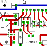
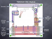
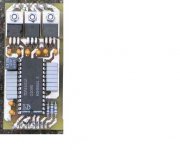
So i only must think about a new TDA1541A, PSU & Regulator PCB to integrate it in his environment as shown in the next picture.
I designed a new PCB for the TDA1541a, cascadable for two, four, eight ore more DAC´s.
The Power Supply is also strict modular with a +/- PS-Board and two Regulator Boards with Salas great Shunt design.
One only for the TDA1541a and the other for the Buffer-IC on the DAC-Board and add. Digital Modules like Doede´s Input PCB´s.
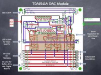
So here are my new modules:
As you could see, the Buffer-IC is completely independent from the DAC power lines!
So you could use a separate regulator for it if you want.
For the Output-Stage i will connect my Tube-I-zator PCB, but everything else is surely possible.
After days of drawing the new PCB´s, i must relax a bit before the next step begins, the production of the PCB´s.
Many thanks to Doede Douma for his brilliant concept and to Salas for his outstanding regulator design.
Best regards to the community,
Oliver

Unfortunately not with a ready build PCB. So i decide to make a new DAC project with this main goals:
- Modular architecture to get max. flexibility
- DAC cascadable
- Compl. I2S-BUS architecture
In the modular design i see the main advatage. Every stage could be build upon the requirements:
- Input section
- DAC section
- Output section
- PS section
- Regulator section
This idea is surely not new. Doede Douma made a perfect modular system with his DDDAC 1543 MKII on his side.
He had the same goals but build his DAC only around the TDA1543.
His Input section with a separate USB to I2S PCB and SPDIF to I2S PCB, both with precise TentLab low jitter clocks, are superb.
So i only must think about a new TDA1541A, PSU & Regulator PCB to integrate it in his environment as shown in the next picture.
An externally hosted image should be here but it was not working when we last tested it.
I designed a new PCB for the TDA1541a, cascadable for two, four, eight ore more DAC´s.
The Power Supply is also strict modular with a +/- PS-Board and two Regulator Boards with Salas great Shunt design.
One only for the TDA1541a and the other for the Buffer-IC on the DAC-Board and add. Digital Modules like Doede´s Input PCB´s.
So here are my new modules:
An externally hosted image should be here but it was not working when we last tested it.
As you could see, the Buffer-IC is completely independent from the DAC power lines!
So you could use a separate regulator for it if you want.
An externally hosted image should be here but it was not working when we last tested it.
An externally hosted image should be here but it was not working when we last tested it.
For the Output-Stage i will connect my Tube-I-zator PCB, but everything else is surely possible.
After days of drawing the new PCB´s, i must relax a bit before the next step begins, the production of the PCB´s.
Many thanks to Doede Douma for his brilliant concept and to Salas for his outstanding regulator design.
Best regards to the community,
Oliver
This is what I am looking for.
TDA1541 module should be able to stack to 2X, 4X or 8X........
External Dem-clock fit into Pin16 and 17 of this modular design will be perfect.
I have 10 TDA1541A sitting here for this project.
The PCB layout underneath of the TDA1541A should be improve, please check with the layout from those manufacturers as a reference.
Last edited:
This is what I am looking for.
TDA1541 module should be able to stack to 2X, 4X or 8X........
If the external Dem-clock Pin16 and 17 can fit into this modular design will be perfect.
That would be no problem. I have a little space to insert a connector for that.
Attachments
The PCB layout underneath of the TDA1541A should be improve, please check with the layout from those manufacturers as a reference.
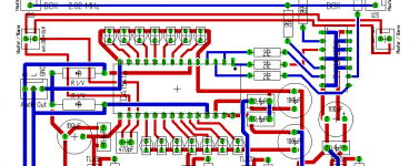
I have forgot to say that all boards become a ground plane on the upper side of the 2-layer design.
So there is a optimal shield between the upper (blue) and base (red) layer.
That would be no problem. I have a little space to insert a connector for that.
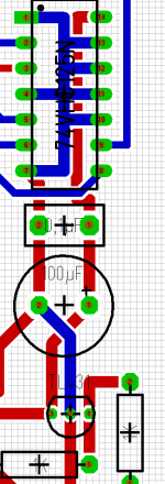
One base board with the external dem-reclock and I2S with indepand supply.
stackable TDA1541A over the base board
Attachments
I have forgot to say that all boards become a ground plane on the upper side of the 2-layer design.
So there is a optimal shield between the upper (blue) and base (red) layer.
Believe me, there must be a reason that all manufacturer's TDA1541A layout looks almost the same. Stick with it!!!!!!!!
Last edited:
One base board with the external dem-reclock and I2S with indepand supply.
stackable TDA1541A over the base board
So this must be better...
Attachments
Perhaps it is a good idea to integrate the DEM clock circuit on the Module?
That is what I have sugessted on thread #5
One base board with the external dem-reclock and I2S with indepand supply.
stackable TDA1541A and power supply modules over the base board
The base board module will supply power line, the dem-reclock and I2S signals to stackable TDA1541 modules.
Last edited:
why not all the dac but only TDA1541A part
you can make ultimate TDA1541A pcb layout
I don´t understand your question...
@ fastvideo
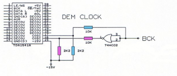
Is this the circuit from ecdesigns that´s in your mind for the DEM-reclock?
This circuit doesn't work well to me, I have to change it this way to work:
with the same ics, 5V supply to both ic, removed D1, D2, R1, R2, R3, R4, R5. signal goes directly to U3 pin1, 2.
Originally Posted by -ecdesigns-
connecting pin 16 to -15V through a 2K2 resistor, and pin 17 to -15V using a 2K2 resistor. The DEM signal can then be injected using 10K Ohm between inverted and non-inverted DEM clock pin 16, and inverted DEM clock pin 17.
Last edited:
So we have this schematic! But if we have more than one board, how is the connection than? Should i insert this schematic on the module, so every 1541A has it´s own or extenal (one re-clock circuit for all DAC´s)?
What´s about the I2S attenuator? Is it still necessary in a buffered input like on my module?
What´s about the I2S attenuator? Is it still necessary in a buffered input like on my module?
Attachments
Last edited:
So we have this schematic! But if we have more than one board, how is the connection than? Should i insert this schematic on the module, so every 1541A has it´s own or extenal (one re-clock circuit for all DAC´s)?
What´s about the I2S attenuator? Is it still necessary in a buffered input like on my module?
I would go this way:
Base PCB. Power line, Dem-reclock and I2S attenuator. (May be it can have the first TDA with it)
Then the TDA1541 portion will be on a smaller stackable PCB. (The missing portion of your original)
One on top of the other one, I think this is the shortest path.
Attachments
Last edited:
That would be one way, yes. But with the shunt regulators for each power line, you don´t get it much smaller.
Think about a 8x TDA, than we would have a skyscraper witch won´t fit in any case.
The outline of this module is about 125x125mm, so a compact design. As i posted before,
i won´t change my base concept. So i will try to insert the DEM-reclock, but will the 74HC02 drive all DAC´s on it´s output,
or do we have a 74HC02 for each DAC´s if we use more than one?
Do you have some experiences with the I2S attenuator after the buffer? I don´t know if it is necessary after it.
Last edited:
- Status
- This old topic is closed. If you want to reopen this topic, contact a moderator using the "Report Post" button.
- Home
- Source & Line
- Digital Line Level
- My take to the "Reference" TDA1541A DAC with I2S-BUS architecture