Hi Guys,
I'll attach the measurements in three different sets. One for the classic arrangement, one for the modified (16 ohm source resistors) version, and a final one to show the FFT at various digital input levels.
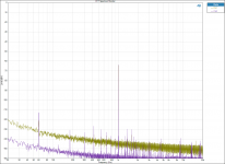
Let's start with the classic version:
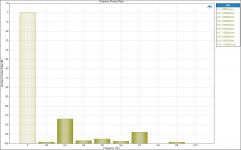
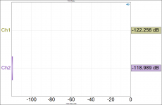
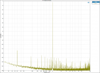
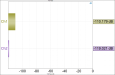
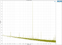
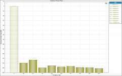
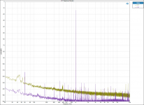
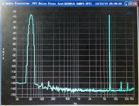
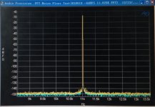
THD is roughly -122dB at -9dBFS and about -114dB at 0dBFS.
At -9dBFS, the third harmonic is down about 130dB and the second is down about 138dB.
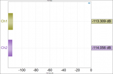
At 0dBFS, the third harmonic creeps up to about -114dB and the second harmonic stays down at around -138dB.
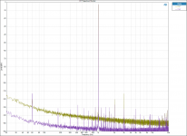
Please not that the 60Hz hash seen in the FFT is caused by the non isolated Arduino controller I recently added. I'm awaiting an ADI isolator for the two I2C lines so I can break the ground between both boards.
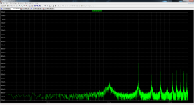
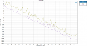
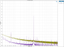
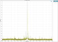
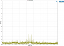
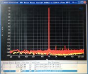
Next up, there is a comparison FFT between the classic arrangement and the new one with the 16 ohm resistor.
The last graph is from the simulation I ran for the NTD1 in classic arrangement. It correlates pretty well!
More to follow...
I'll attach the measurements in three different sets. One for the classic arrangement, one for the modified (16 ohm source resistors) version, and a final one to show the FFT at various digital input levels.
Let's start with the classic version:
THD is roughly -122dB at -9dBFS and about -114dB at 0dBFS.
At -9dBFS, the third harmonic is down about 130dB and the second is down about 138dB.
At 0dBFS, the third harmonic creeps up to about -114dB and the second harmonic stays down at around -138dB.
Please not that the 60Hz hash seen in the FFT is caused by the non isolated Arduino controller I recently added. I'm awaiting an ADI isolator for the two I2C lines so I can break the ground between both boards.
Next up, there is a comparison FFT between the classic arrangement and the new one with the 16 ohm resistor.
The last graph is from the simulation I ran for the NTD1 in classic arrangement. It correlates pretty well!
More to follow...
Attachments
-
 DPR 0dBFS classic NTD1.png50.1 KB · Views: 1,110
 -
 FFT Spectrum Monitor compare.png135.2 KB · Views: 192
 -
 THD -9dBFS classic NTD1.png42.3 KB · Views: 958
 -
 THD 0dBFS classic NTD1.png43.7 KB · Views: 1,057
 -
 FFT -9dBFS classic NTD1.png109.3 KB · Views: 1,075
 -
 DPR -9dBFS classic NTD1.png49.2 KB · Views: 1,079
 -
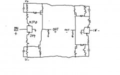
 NTD1 400R bipolar supply.png126.7 KB · Views: 219
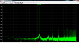
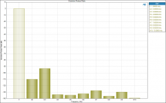
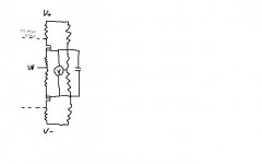
Next up is the modified version with the 16 ohm source resistors and single positive supply.
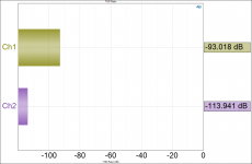
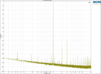
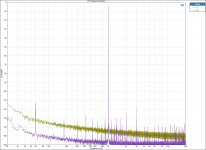
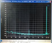
THD for the modified design sits at -93dB for 0dBFS and -110dB for -9dBFS. Both very respectable, but about 10 to 20dB worse than the classic arrangement.
At 0dBFS, the 3rd harmonic climbs up to -94dB with the second sitting at -110dB.
Dropping back to -9dBFS things improve quite a bit with the 3rd harmonic down at -113dB and the 2nd at -120dB
Last up is the simulation which again is pretty close to reality!
Overall, I would only suggest this modification if you really are hurting for power dissipation, and can live with the higher THD. It's actually a pretty fair trade-off performance wise, but if you're looking for the best possible performance, stick with the classic arrangement!
Next up is the measurements requested by bbp.
Attachments
-
 NTD1 15R single supply.png143.1 KB · Views: 136
 -
 THD -9dBFS MOD CAP NTD1.png43.8 KB · Views: 99
 -
 THD 0dBFS MOD CAP NTD1.png44.3 KB · Views: 102
 -
 FFT -9dBFS MOD CAP NTD1.png111.6 KB · Views: 102
 -
 FFT 0dBFS MOD CAP NTD1.png109.9 KB · Views: 109
 -
 DPR -9dBFS MOD CAP NTD1.png50.4 KB · Views: 106
 -
 DPR 0dBFS MOD CAP NTD1.png52.2 KB · Views: 190
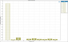
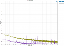
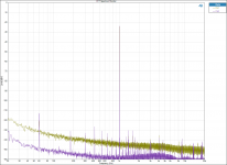
Finally we've got the FFTs for different input digital levels.
Overall, everything is pretty consistent regardless of input level.
Cheers,
Owen
Overall, everything is pretty consistent regardless of input level.
Cheers,
Owen
Attachments
-
 THD+N Ratio vs level.png71.7 KB · Views: 108
 -
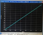
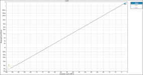 Gain linearity.png55.2 KB · Views: 113
 -
 FFT Spectrum Monitor -70.png137.1 KB · Views: 92
 -
 FFT Spectrum Monitor -60.png135.7 KB · Views: 90
 -
 FFT Spectrum Monitor -50.png130.9 KB · Views: 103
 -
 FFT Spectrum Monitor -40.png132.5 KB · Views: 97
 -
 FFT Spectrum Monitor -30.png136 KB · Views: 104
 -
 FFT Spectrum Monitor -20.png131.5 KB · Views: 124
 -
 FFT Spectrum Monitor -10.png138.1 KB · Views: 154
Hi Owen,
thank you very much for the informations.
I also will stick with the classic circuit.
You know I don´t use 200R /400R
Because my Aleph-X amp needs high input level, I changed my configuration to 400R / 750R and I am happy with it. Distortion stays low.
I get much less heat and 6dB more output level (twice the amount).
Its a alternative for builder who have probems with the heat.
Maybe you can make a simulation with this values and compare the distortion of 400R/ 750R vs 200R/ 400R
Please make the simulation with the same analog output levels, not the same input level. With the same input level you will get twice the distortion because you get twice the output level.
Finally we've got the FFTs for different input digital levels.
Overall, everything is pretty consistent regardless of input level.
Cheers,
Owen
Hi Owen,
Thank you thank you so much!
Thanks for your effort about the measurement. I think this performance is good enough for most of the audiophiles!
But to the THD+N vs. Output level, I think I must pay more attention to this spec. Many abnormal ripple ripple still can be seen in that curve.
Thanks again!
Have a nice day!
Paul
Hi bbp,
I wouldn't put much weight on that measurement. It's really only to show the general trend. It's a single unit measure (one number to describe all THD+N) plotted over output level, which tends not to show the whole picture.
The AP has a tendency to need a lot of settling time when taking sweeps like the one shown, and it was only set to default, so that's more than likely why you're seeing the peaks in that measurement. I can repeat it on Monday with a longer settling time and it would probably be more linear.
The FFT measurements are the ones I really wanted to relay. They are far more accurate and detailed accounts of what is actually going on.
Take a look at these for example, which show the effects of jitter in the analog domain")
Cheers,
Owen
I wouldn't put much weight on that measurement. It's really only to show the general trend. It's a single unit measure (one number to describe all THD+N) plotted over output level, which tends not to show the whole picture.
The AP has a tendency to need a lot of settling time when taking sweeps like the one shown, and it was only set to default, so that's more than likely why you're seeing the peaks in that measurement. I can repeat it on Monday with a longer settling time and it would probably be more linear.
The FFT measurements are the ones I really wanted to relay. They are far more accurate and detailed accounts of what is actually going on.
Take a look at these for example, which show the effects of jitter in the analog domain
Cheers,
Owen
Attachments
Hi bbp,
I wouldn't put much weight on that measurement. It's really only to show the general trend. It's a single unit measure (one number to describe all THD+N) plotted over output level, which tends not to show the whole picture.
The AP has a tendency to need a lot of settling time when taking sweeps like the one shown, and it was only set to default, so that's more than likely why you're seeing the peaks in that measurement. I can repeat it on Monday with a longer settling time and it would probably be more linear.
The FFT measurements are the ones I really wanted to relay. They are far more accurate and detailed accounts of what is actually going on.
Take a look at these for example, which show the effects of jitter in the analog domain
Cheers,
Owen
Got it!
Which I have is an ATS-2 in my hand. It seems that there's a little different in the sweep test to your APx585/525.
Anyway, I am working on my own ES9018 DAC now. Your idea about this IV conversion is so amazing for us.
I also test NTD1 without ES9018 last week. The performance is so good even assembly with a simple breadboard.
A ultra-high performance LDO will be present together with my DAC later ^_^
I will share the whole work with you once the total solution is good enough.
Thank you!
Regards
Paul
opc,
what do you think about that? à la ba-3...
it seems that there is no bias voltage for the Iout of ES9018
bbp,
ah yes you are right...forgot about that. what about a voltage divider that would tie the jfets gate to 1.65v?
i m also not sure if there is idle current also...but maybe a simple ccs would do it?
in fact i wanted to build a pcm1794 I/V and wanted to share ideas, good or bad.
ah yes you are right...forgot about that. what about a voltage divider that would tie the jfets gate to 1.65v?
i m also not sure if there is idle current also...but maybe a simple ccs would do it?
in fact i wanted to build a pcm1794 I/V and wanted to share ideas, good or bad.
bbp,
ah yes you are right...forgot about that. what about a voltage divider that would tie the jfets gate to 1.65v?
i m also not sure if there is idle current also...but maybe a simple ccs would do it?
in fact i wanted to build a pcm1794 I/V and wanted to share ideas, good or bad.
BIAS voltage for every DAC is very very important, the noise in BIAS will be delivered by the output stage directly.
I am working on a ultra-pure ultra fast response voltage regulator, which will be used in my new DAC.
My project
Hi OPC,
Thanks so much about your work and your guide line for us.
My project prototype work is done now, I am gonna share my measurement with you here.
It is a circuit based on a common gate structure like yours. but also, it features in other special points. For example, A pure voltage reference is added, target to get lower noise on the gate of mosfet.
Below is my measurement, it seems that this is the best DAC in non-lope feedback design. It is hard to keep non-feedback design in ultra-low THD+N below -120dB, but I believe my work does. It presents lower THD than a AP signal source. I think I have to use AP 2722 to test the 2nd prototype board.
Thanks again.
Regards
Paul Lu
Hi bbp,
I wouldn't put much weight on that measurement. It's really only to show the general trend. It's a single unit measure (one number to describe all THD+N) plotted over output level, which tends not to show the whole picture.
The AP has a tendency to need a lot of settling time when taking sweeps like the one shown, and it was only set to default, so that's more than likely why you're seeing the peaks in that measurement. I can repeat it on Monday with a longer settling time and it would probably be more linear.
The FFT measurements are the ones I really wanted to relay. They are far more accurate and detailed accounts of what is actually going on.
Take a look at these for example, which show the effects of jitter in the analog domain
Cheers,
Owen
Hi OPC,
Thanks so much about your work and your guide line for us.
My project prototype work is done now, I am gonna share my measurement with you here.
It is a circuit based on a common gate structure like yours. but also, it features in other special points. For example, A pure voltage reference is added, target to get lower noise on the gate of mosfet.
Below is my measurement, it seems that this is the best DAC in non-lope feedback design. It is hard to keep non-feedback design in ultra-low THD+N below -120dB, but I believe my work does. It presents lower THD than a AP signal source. I think I have to use AP 2722 to test the 2nd prototype board.
Thanks again.
Regards
Paul Lu
Attachments
-
 DIY AUDIO 50+7K IMD.jpg294.3 KB · Views: 138
 -
 DIY AUDIO 19K+20K IMD.jpg280.2 KB · Views: 128
 -
 DIY AUDIO 15K FFT.jpg238.5 KB · Views: 151
 -
 DIY AUDIO 7K FFT.jpg255.3 KB · Views: 185
 -
 DIY AUDIO 1K FFT.jpg252.2 KB · Views: 1,031
 -
 DIY AUDIO 50HZ FFT.jpg195.3 KB · Views: 1,061
 -
 DIY AUDIO JITTER.jpg107.2 KB · Views: 1,083
 -
 DIY AUDIO LINEARITY.jpg155.6 KB · Views: 1,141
 -
 DIY AUDIO 1K FFT VS AP.jpg218.3 KB · Views: 166
Last edited:
bbp can you share your circuitry?I want to know how you improve. Thank you!
Sorry, Chen. I am trying to write a PAT. on it.
I think it is possible to do this.
In my measurement, the negative kick from Source point will be < -10V sometime when I power the original NTD1 off. I think no Zener can protect ES9018 from such a high kick.
bbp:
It's a little hard to get a read on the intentions of your posts, but I'm not getting a very warm and fuzzy feeling from the last few things you wrote.
There are a few basic etiquette items you're not respecting:
1. You've hijacked a thread to show results from your "modified" circuit, claiming it's a large improvement, and then not sharing the actual circuit. What was your reason for doing this? How is this information relevant to anyone in this thread if you don't share the underlying circuit?
2. You've made a claim that your circuit is achieving better performance, when it's actually a little bit worse. The noise floor looks to be higher, and the distortion is also higher than a standard NTD1.
3. You're claiming that the NTD1 is going to damage an ES9018 when this is not the case. The NTD1 is a thoroughly tested and widely used circuit. Mine has been in constant service for several years and is still performing perfectly. I have posted measurements way back in the thread of the voltage swing on the output of the DAC (source of the fets) during startup and shutdown, and there is no risk of damage with a properly built and adjusted NTD1, with or without the zener diodes. Please don't make completely false and unsupported claims that the NTD1 will harm the DAC.
As for the patent, I think you might be getting a little ambitious. It's essentially impossible for an individual to foot the bill for a patent application and the subsequent legal muscle required to protect it. This of course is in addition to the fact that I strongly doubt there is any new art to be had in this area. A better voltage source on the gate is hardly groundbreaking and not really a deviation from the existing circuit. Add to this the fact that performance is worse, and you're not looking at much of a patent application.
Forgive me if I've misunderstood the intentions of your posts, and I don't mean to be overly harsh, but this forum is all about the sharing of information for the betterment of everyone's knowledge and personal listening experience. After all, it's how you found this circuit in the first place isn't it? Tis the season for more giving and less taking!
Regards,
Owen
bbp:
It's a little hard to get a read on the intentions of your posts, but I'm not getting a very warm and fuzzy feeling from the last few things you wrote.
There are a few basic etiquette items you're not respecting:
1. You've hijacked a thread to show results from your "modified" circuit, claiming it's a large improvement, and then not sharing the actual circuit. What was your reason for doing this? How is this information relevant to anyone in this thread if you don't share the underlying circuit?
2. You've made a claim that your circuit is achieving better performance, when it's actually a little bit worse. The noise floor looks to be higher, and the distortion is also higher than a standard NTD1.
3. You're claiming that the NTD1 is going to damage an ES9018 when this is not the case. The NTD1 is a thoroughly tested and widely used circuit. Mine has been in constant service for several years and is still performing perfectly. I have posted measurements way back in the thread of the voltage swing on the output of the DAC (source of the fets) during startup and shutdown, and there is no risk of damage with a properly built and adjusted NTD1, with or without the zener diodes. Please don't make completely false and unsupported claims that the NTD1 will harm the DAC.
As for the patent, I think you might be getting a little ambitious. It's essentially impossible for an individual to foot the bill for a patent application and the subsequent legal muscle required to protect it. This of course is in addition to the fact that I strongly doubt there is any new art to be had in this area. A better voltage source on the gate is hardly groundbreaking and not really a deviation from the existing circuit. Add to this the fact that performance is worse, and you're not looking at much of a patent application.
Forgive me if I've misunderstood the intentions of your posts, and I don't mean to be overly harsh, but this forum is all about the sharing of information for the betterment of everyone's knowledge and personal listening experience. After all, it's how you found this circuit in the first place isn't it? Tis the season for more giving and less taking!
Regards,
Owen
Hi Owen,
I am sorry about showing the measurement in your thread. I will delete the measurement post later to avoid misunderstood.
The fist time I post measurement here is intend to share the result together with the circuits. But as my work goes on, I made a miracle circuit based on common gate structure which is also used in NTD1. The new circuit presents miracle -140dB THD and my AP system can not measure the real distortion! The output voltage as high as 30Vrms with 120v VDD. That's why I have no post my circuit and share with you guys at last.
The original NTD1 is great, we're no doubt about that. No other simple circuit can presents such a low THD for IV use in the world except NTD1. That's why I give my thanks to you many times, for you share such a great circuit with us. Thanks again ^_^
But the output voltage is limit for a standard balance output DAC, only ~2Vrms for 100kohm load. That's I have to modify it. Simply increasing the 200R is not the best option, because large R means large voltage swing on Vds of MOSFET, which will cause larger non-linear for the output signal. The original design by you is nearly the best! Because you pay lots of time to work out NTD1.
For the damage, I can see no out of function damage for my ES9018 with NTD1, but I think the several voltage negative kick do have degraded its original performance.
In my simulation based on NTD1 which generous post by you, the negative kick during power-on/power-off is real. In my bench test, the kick is also real. I will give my appologize to you in case you can post the real non-negative kick measurement waveform with us later.
Have a nice weekend.
regards
Paul
- Status
- This old topic is closed. If you want to reopen this topic, contact a moderator using the "Report Post" button.
- Home
- Source & Line
- Digital Line Level
- A New Take on the Classic Pass Labs D1 with an ESS Dac