errmm good suggestions, but we really dont want to turn this into another thread and start the design all over again. real results from the last schematic are good enough for me and at the boundaries of all but the best test equipment. and the sound is excellent, I just would like something with a more suitable design without so many alterations to fit the current schematic
I would hate for owen to get bombarded with multitudes of different opinions again and decide its too much of a PITA and he cant please everyone, which I could understand, considering he already has a working build. nothing wrong with a bit of feedback, but suggestions to turn it upside down, may not be productive at this juncture
also your calc for caps seem to be completely discounting phase distortion which has effects at up to 10x the corner
Hi pidesd,
IMO Balanced with caps is without a question going to be magnitudes better than a transformer coupled variant.
I'm sure others might disagree, but feel that transformers in the signal chain is about the worst thing you could possibly do to your audio. They distort, they have FR anomalies, they're very source and load dependent, they're expensive, bulky, susceptible to magnetic coupling, and just generally a bad idea unless absolutely necessary.
I know there are some people that swear by them, and even some who run their buffalo DACs in voltage mode directly into a transformer, and then rave about the results, but I can assure you they don't work well, and especially not in the setup I just mentioned.
Just my opinion, but I do have measurements to back it up.
Cheers,
Owen
Hi Owen
I'd just like to say that the layout in post #250 looks spot on, very tidy. I agree with qusp that you shouldn't get bogged down with too many alterations and adjustments.
Can I ask, have you designed the board so that long pin headers are used to connect I/V board to DAC like TP do?
If so, would it be possible to include these in any component GB's that may happen?
Cheers
I actually quite liked the sound of them sometimes and ran TX at the output of the buff for quite a while. definitely not the best measuring or linear and while quite easy to listen to, if going for high resolution and low distortion you can forget about it.
seems like an elegant solution due to the low component count, but if you think of the nasties and how long and massive the circuit becomes it becomes not so appealing. bested by a number of other output stages.
that being said, I would love love love to get rid of those caps, which arent exactly pretty either. though what goes there can easily be left up to the individual.
Last edited:
Hi Guys,
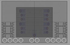
Some more input on pcb layout.
I do not want to look as unapreciative of opc's fantastic work, this is just an atempt to do teamwork.
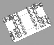
Here is a quick 3D rendering of the major components on opc's initial layout.
3D gives a better "feel" for final product, i think.
Some more input on pcb layout.
I do not want to look as unapreciative of opc's fantastic work, this is just an atempt to do teamwork.
Here is a quick 3D rendering of the major components on opc's initial layout.
3D gives a better "feel" for final product, i think.
Attachments
Last edited:
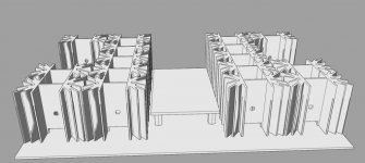
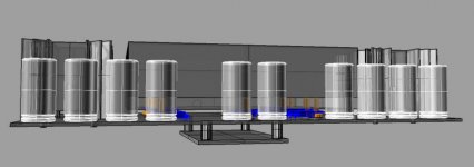
Ilustrating my ealier post on an alternative layout:
This one permits components on both sides of the pcb and leaves more space for coupling caps.
It does mean that DAC is facing down ...but objective is not to look at DAC i think...it's the music")
note: big heatsink is generic, this is just to portray the idea.
This one permits components on both sides of the pcb and leaves more space for coupling caps.
It does mean that DAC is facing down ...but objective is not to look at DAC i think...it's the music
note: big heatsink is generic, this is just to portray the idea.
Attachments
Last edited:
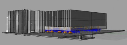
If everything will be integrated in one pcb, why not bolt everything down on two large heatsinks on the sides? Then it is possible to bolt some aluminium panels onto the heatsinks to create a nice enclosure.
But then again, Owen, you already said that laying out this circuit with the resistors and mosfets on the sides will be hard, but I just wanted to make this suggestion.
But then again, Owen, you already said that laying out this circuit with the resistors and mosfets on the sides will be hard, but I just wanted to make this suggestion.
If everything will be integrated in one pcb, why not bolt everything down on two large heatsinks on the sides? Then it is possible to bolt some aluminium panels onto the heatsinks to create a nice enclosure.
But then again, Owen, you already said that laying out this circuit with the resistors and mosfets on the sides will be hard, but I just wanted to make this suggestion.
most of us already have enclosures
Guys,
I thought we could discuss ideas here, i'm most definively in for watever is decided here, and yes ( qusp ...got your nik right?) team work means listening to others with some respect ( no wink ).
I was trying a theoretical solution to give opc the option of more availaible pcb space to work with, i was trying to help if there is doubt.
I have no problem in accepting that this option is not acceptable to you guys.
....and still availaible to help if it is deemed usefull.
I came in on this thread because i liked owen's work so much ...if there was doubt.
Last edited:
I suggest that the original layout was a good choice for what many of us would like to use in an enclosure. The thermal design is fairly critical here and should be improved on only by making the board wider by enough to add space between heatsinks for cool air inflow. Adding holes in the board beneath the end of the heatsinks would also be a very good idea. Alternatively, the existing layout with an area routed beneath the ends of the heatsinks - opening the area beneath the fins completely - would work well. This desigh will require a vented enclosure if the final layout does not attach the devices to an external heatsink because of the Pdis.
Thanks for the hard work and best regards,
Dave
Thanks for the hard work and best regards,
Dave
I suggest that the original layout was a good choice for what many of us would like to use in an enclosure. The thermal design is fairly critical here and should be improved on only by making the board wider by enough to add space between heatsinks for cool air inflow. Adding holes in the board beneath the end of the heatsinks would also be a very good idea. Alternatively, the existing layout with an area routed beneath the ends of the heatsinks - opening the area beneath the fins completely - would work well. This desigh will require a vented enclosure if the final layout does not attach the devices to an external heatsink because of the Pdis.
Thanks for the hard work and best regards,
Dave
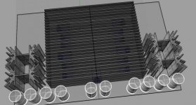
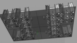
would something like this work fitzfish:
Attachments
Guys,
I thought we could discuss ideas here, i'm most definively in for watever is decided here, and yes ( qusp ...got your nik right?) team work means listening to others with some respect ( no wink ).
I was trying a theoretical solution to give opc the option of more availaible pcb space to work with, i was trying to help if there is doubt.
I have no problem in accepting that this option is not acceptable to you guys.
....and still availaible to help if it is deemed usefull.
I came in on this thread because i liked owen's work so much ...if there was doubt.
yeah you got it right mate thanks, its from a fantastic Greg Egan book, people get it wrong all the time because even though we are conditioned to all sorts of misspelt and crazy nicks, people just cant seem to bring themselves to put a u after a q without a vowel after it; even though its staring them in the face
quasp and quisp are popular alternativeshey look, I have no issue with you trying to help, in fact its appreciated. but at this late stage I think you gotta draw the line as to what exactly is helpful. this thread has been around for well over a year with no result (as far as a PCB anyway, as the design works quite well) for a number of reasons. the design is in place, the parts are in place, the specs are excellent!!, the sound is excellent!!, finalizing the PCB layout for heatsinking is really the only thing left to do. Changing the design and entering into power supply discussions is not going to help that. suggestions at this stage to rework it to such a degree including literally turning the thing upside-down; arent really what I would call productive towards that end.
we could also add a sophisticated MUX with spdif to i2s convertor, discrete shunt regulated power supply and an MCU for volume control/input switching, but that wouldnt be productive at this stage either. these are the sort of things people can add themselves if they wanna take it that far
wasnt being disrespectful; facetious yes, disrespectful? not so much. sorry if I offended you
I have to kind of take a bit of a back seat here, because even though initially this was going to be designed with the ackodac in mind as the platform, OPC ended up buying himself a buff II; most likely due to impatience waiting for the ackodac to be finished (totally understandable as it was a long time coming, but it was a bit frustrating for me), so the direction changed for best fit with the buff both physically and WRT power supply. I run a buff II portable, but my home dac is an ackodac, so i'll have to live with a less than perfect fit and I dont mind that, but totally unusable without massively long signal connections doesnt thrill me, I may as well stick with what I have.
I have a feeling that the above would be impossible to route the traces around, but otherwise sure and if some of those holes could be in the right place for screwing the components down on the floor for those who wish to do that, that would work.
Hi qusp,
you just confirmed my liking for australians, love the plave, love the people.....
the main reason i posted the above rendering was exactly to ilustrate where we should or should not put holes.....as it is shown it's a ver holy board....pun intended.
but not very easy to route around as you say.
Realistically i think we should place holes only beneath the heatsink wings, this would ease the routing issue to the transistors and resistors while permiting better air flow to the heatsinks.
Last edited:
- Status
- This old topic is closed. If you want to reopen this topic, contact a moderator using the "Report Post" button.
- Home
- Source & Line
- Digital Line Level
- A New Take on the Classic Pass Labs D1 with an ESS Dac