Hi Bunpei,
Thank you very much for your continued support!
I am actually preparing to test the SDTrans384. The Turbo Clock is directly compatible, so minimal mods required. But first I need to get an interface board done that will take the header outputs of the SDTrans and fan out to w.fl coax to match the AKD12 Digital Inputs.
This is almost ready but I have noticed that when physical connections are arranged for DSD from SDTrans, the DAC inputs will not be compatible with I2S (stereo mode). This means I cannot play pcm audio on a DAC setup for DSD and vice versa, unless the digital inputs are physically reconnected to match. The line of contention is LRCK (of I2S) that becomes DSD1 and also the way the DAC cells are connected to the inputs.
Not sure if I am getting confused with all the signal lines but any help is most appreciated.
Not sure if it will tell you anything you dont know but have you had a look at the Hifiduino site?
The Amanero USB board seem to be able to change the outputs to fit the ESS inputs. Not sure how it is done, but the outputs are configured correctly with both DSD and PCM but that is done at the source (amanero board). Edit: that internal switching of the ESS chips will give most people a headache...
Edit2: could the outputs from the source be altered in firmware to output DSD in one manner and PCM in another (based on source material)?
Last edited:
not as simple as that and it wasnt solved with arduino, amanero had to have its firmware modified. amanero simply had left and right channels of DSD switched when wired to PCM standard wiring, the problem here is with the sdtrans board and the way it is wired afaik and no code or function of ESS can fix that.
... to match the AKD12 Digital Inputs ...
This is almost ready but I have noticed that when physical connections are arranged for DSD from SDTrans, the DAC inputs will not be compatible with I2S (stereo mode). This means I cannot play pcm audio on a DAC setup for DSD and vice versa, unless the digital inputs are physically reconnected to match. The line of contention is LRCK (of I2S) that becomes DSD1 and also the way the DAC cells are connected to the inputs.
Dear Acko,
I'm not sure about input configuration scheme of AKD12.
The output pin assignments of SDTrans are;
LRCK ... DSD Left
SDAT ... DSD Right
DCLK ... DSD DCLK
(MCLK ... Master Clock Output)
when SW1-1 OFF, SW1-2 ON (Both PCM, DSD are available)
This assignment fits TPA Buffalo II input style well without any physical re-wiring upon switching between DSD and PCM.
"glt" gives us a very clear explanation of the input configuration scheme on his blog page;
Hifiduino Code and Buffalo III DAC H i F i D U I N O
Please remember that register setting for ES9018 to enable input re-mapping is necessary.
Best regards,
Bunpei
Last edited:
DSD
Thank you all.
Yes, that is what I thought, inputs must be either reconnected physically or remapped using the quantizer bits. Setting quantizer bits (reg#15) is not even mentioned in the datasheet, so I was going with the standard connections. For the AKD12 there are no jumpers or switches. Input connections are : DATA1 -DAC1 .... DATA8-DAC8. For stereo I2S, DATA1,2,3 & 4 lines are connected to I2S SDATA line to fill all the 8 DACs and the arrangement of the internal DAC cells nicely takes care of L/R outputs.
For stereo DSD, I was trying to connect DATA1, DATA3, DATA5 and DATA7 to DSD1 output from SDTrans. This will form the RIGHT Channel of the DAC
Then DATA2, DATA4, DATA6 and DATA8 to DSD2 output of SDTrans for LEFT Channel. Again no problem with DSD stereo on its own but you will see that it will jumble up I2S
Will check out GLT's site also, very informative! Thank you GLT
Super Trans
No problems, just stayed tuned")
Just got FIFO-Clock (and freebies) for evaluation from Ian today. Trying to get my head around all the bits now
Acko, I'm just stirring the pot there mate.
No problems, just stayed tuned
Just got FIFO-Clock (and freebies) for evaluation from Ian today. Trying to get my head around all the bits now
Hi there AR2, great work.
Could you point me to further information on the jfet buffers you are using ?
Thank you deanoUK.
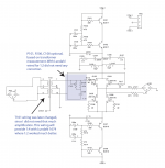
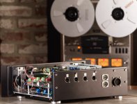
Here is the schematic of buffers I am using. I posted picture and PDF, so it is easier to read for you. Buffer could be stand alone, without trafo, but together it was intended and used as an output stage for voltage out DACs, particularly AK4396. It is an outstanding unit and very versatile. As you could see there are no caps in the line of signal, and any DC coming out of DAC is blocked by Lundahl. Originally it was designed to be 1+1 : 4+4 but that was too much and I am using it as 1 +1 : 2 + 2. That also gives much less distortion.
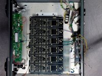
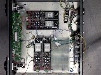
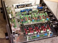
Here are some shots of populated boards as well as empty ones, and some of many implementations I did in the process of making my DAC. I do not have any more boards, but if you would like to make your own I will be happy to send you gerber files.
Attachments
Yes, that is what I thought, inputs must be either reconnected physically or remapped using the quantizer bits. Setting quantizer bits (reg#15) is not even mentioned in the datasheet, so I was going with the standard connections.
I'm afraid that you have misunderstood the input re-mapping mechanism somehow. I think no quantizer setting on Register #15 is essential. Instead, "Register #14: DAC3/4/7/8 Source" settings are necessary.
Anyway, AKD12 might have a "ESS Evaluation Board" type simple input terminals. In this case, you may need a few bridging before you connect lines to AKD12 input.
To glt, would you give your comments?
No problems, just stayed tuned
Just got FIFO-Clock (and freebies) for evaluation from Ian today. Trying to get my head around all the bits now
if you need any help dont hesitate to ask
I'm afraid that you have misunderstood the input re-mapping mechanism somehow. I think no quantizer setting on Register #15 is essential. Instead, "Register #14: DAC3/4/7/8 Source" settings are necessary.
Anyway, AKD12 might have a "ESS Evaluation Board" type simple input terminals. In this case, you may need a few bridging before you connect lines to AKD12 input.
To glt, would you give your comments?
I think it will have the same effect. The correct way is to remap with reg14, if using reg15 you will be limited to 8bit and 9bit
Thanks Qusp, will do.if you need any help dont hesitate to ask
Actually couple already. Thought FIFO-Dual clock was capable of 384KHz but leds on the Dual Clock indicating up to 192KHz only. And then the isolator board, if inserted after the FIFO wouldn't it introduce additive jitter going through all the GMRs?
Speeds higher than 192 are indicated by combination of LEDs, I'm away from my comp at the moment but I am sure Ian has the combinations in the docs
All i2s lines are reclocked with the potato logic flipflops at output of the clock board so GMR additive jitter has no impact unless it misses the clock cycle input to the flipflop, if that was the case Ian's bit perfect tests would fail I expect. Delay through the flipflop should be the only jitter seen at the output which is how Ian comes up with his ~2ns spec.
All i2s lines are reclocked with the potato logic flipflops at output of the clock board so GMR additive jitter has no impact unless it misses the clock cycle input to the flipflop, if that was the case Ian's bit perfect tests would fail I expect. Delay through the flipflop should be the only jitter seen at the output which is how Ian comes up with his ~2ns spec.
Last edited:
acko,
Ian described the re-clocking briefly here:
Ian described the re-clocking briefly here:
Both of the clock board and I2S to PCM convertor board re-clock the I2S at last stage, in this case, only jitter from MCLK is significant. Dont worry about the signal path, additional jitter will be re-clocked anyway.
Ian
Speeds higher than 192 are indicated by combination of LEDs, I'm away from my comp at the moment but I am sure Ian has the combinations in the docs
Looked at V1.0 docs for both FIFO and Dual Clock. Nothing going beyond 192KHz in the specs.
I know Ian confirmed 384KHz capability somewhere but can't remember which doc it was.
Looked at V1.0 docs for both FIFO and Dual Clock. Nothing going beyond 192KHz in the specs.
I know Ian confirmed 384KHz capability somewhere but can't remember which doc it was.
I just found it, you're right its a bit of a search mission to work out where it is. It's in the dualXO board docs from GBII. Doc attached here - http://www.diyaudio.com/forums/grou...s-pdif-fifo-kit-group-buy-40.html#post3093337
Thanks Qusp, will do.
Actually couple already. Thought FIFO-Dual clock was capable of 384KHz but leds on the Dual Clock indicating up to 192KHz only. And then the isolator board, if inserted after the FIFO wouldn't it introduce additive jitter going through all the GMRs?
thats OK, the 384 is indicated by both lit from memory, it was not initially designed for indicating such high speeds but copes no problem with latest FW. you could also look at using a little BGA sink on the FPGA
hochopeper has it pretty much right.
at my prompting
the isolator board was designed to go between the fifo main board and clock board very deliberately. this way you even isolate the clock board from the possible slew and simultaneous switching noise from the FPGA and all that PC related ripple that comes before it if USB->i2s is used. this places it at the last point before the reclock stageEffectively it allows the clock board to be married to the dac again. then its reclocked by the dual clock board + flip flops, effectively deleting the jitter from the isolator as well as that before it; aside from the XO + buffer self noise/jitter
initially the parts on the dual clock board were potato logic, but I think he changed to Ti for later versions of that board, changing back to potato logic for the si570 with more knowledge gained on their use. thats how it was anyway, perhaps he has changed back again on the dual XO too.
a possible experiment that I will do and perhaps you can too, is to power the output side/quiet side of the isolator and the clock buffers with the same power supply (or one that is grounded on the dac side ground plane directly) as is powering the logic/ring of the ESS dac. cant remember if its that specific, or just the same ground, same PSU, so could be any of them, even a beefed up flea with mosfet grounded/connected where the old (presumably now vacant/unused) clock reg was perhaps? just an idea
I believe EXA uses this technique too, this apparently helps with lower asynchronous mode DPLL bandwidth stability and has something to do with the star grounding, which if we are honest does seem to be a bit of a sticky point with the ESS dacs yes? they seem more easily disturbed by ripple on ground and their digital supply than you would think (only apparent when shooting for lowest DPLL, not 'best' defaults
alternatively a you could also reinforce the ground connection between the boards, with buss bar or something, though you would preferably use some way that didnt negate the vibrational decoupling.
Not that with the high clock speeds the fifo needs much help there and with sync mode its not really relevant, maybe worth some playtime though, if there is any possible way to discern the difference.
is that a satisfactory answer? =)
Last edited:
Acko, I know AKT is probably mostly aimed at the higher grade ESS chips. I have worked out a nice integration technique for the AKD23P though.
Ian's FIFO board has a silence output on J13, this is active high, so will need to be run through an inverter then to the general purpose isolator on its way to the MuteB pin on the ES9023. This will hopefully allow DAC noises and any noise during XO selection to be suppressed.
For the cost of a TTL inverter I think this would be pretty nice to have for the extra polish.
My AKD23P makes almost no noises during turn on in my current system, I'm not sure of it's behaviour with the FIFO though (waiting on next GB) so this isn't a problem per se but since Ian's already done the hard work, it would make sense for it to be used, right?
Chris
is that a satisfactory answer? =)
Thanks Qusp, points noted.
I have got the latest manuals and boards from Ian also. The Clock board is marked DoublerateDualClock with FW3.3. At first blush showing up to 352KHz only. Cannot seem to find the 384KHz rates. Not trying to be pedantic but I have plans to tap all these bits and direct them to an I2C comms chip on my upcoming SuperTrans module so that the Controller (AKC12) or Arduino can read them. As pointed out by GLT, in Sync mode the Sabre DAC gets disorientated trying to figure out sample rates by itself, so getting it direct from transport is the way to go.
Ian's FIFO board has a silence output on J13, this is active high, so will need to be run through an inverter then to the general purpose isolator on its way to the MuteB pin on the ES9023. This will hopefully allow DAC noises and any noise during XO selection to be suppressed.
For the cost of a TTL inverter I think this would be pretty nice to have for the extra polish.
Chris
It would a good thing to do for overall mute. Possibly simpler to kludge an open collector BJT (straddle the mute header of the AKD23)
Ok, found it now, LED for Fs=192KHz indicates 384KHz in double speed mode.At first blush showing up to 352KHz only. Cannot seem to find the 384KHz rates.
- Status
- This old topic is closed. If you want to reopen this topic, contact a moderator using the "Report Post" button.
- Home
- Source & Line
- Digital Line Level
- ackoDAC based on ES9018