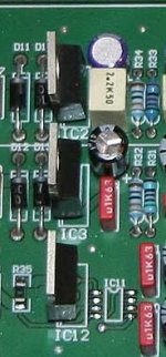
In the "analog supply" section:
IC1 = LM317
IC4 = MC7815C
IC5 = MC7915C
IC6 = LM337
The three stabilizers at the bottom, vertically in line with the "analog output stage":
IC2 = 1587AT, on top of that is printed D49AB
IC3 = 1587AT, on top of that is printed D49AB
IC12 = 1587AT33, on top of that is printed DG7AB
To the right of that, just above where it says "digital supply" and there is the silkscreened area saying "north star design model 192" etc. there are 4 seemingy identical ones labeled as follows:
IC8 = LF50C4, underneath that is GK0TV VW, underneath that is CHN624
IC7 = LF50C4, underneath that is GK0TV VW, underneath that is CHN624
IC10 = LF50C4, underneath that is GK0TV VW, underneath that is CHN624
IC9 = LF50C4, underneath that is GK0TV VW, underneath that is CHN624
xenithon said:In the "analog supply" section:
IC1 = LM317
IC4 = MC7815C
IC5 = MC7915C
IC6 = LM337
No mysteries here.
LM317/337 are adjustables. Judging by the resistors (if I read the colours correctly) they seem to be set to either + and -1.5 V or about + and - 7 V.
Both sets presumably make symmetrical power supplies, e.g. the 7915 and 7815 together form -15 V and +15 V with GND as 0 V.
The three stabilizers at the bottom, vertically in line with the "analog output stage":
IC2 = 1587AT, on top of that is printed D49AB
IC3 = 1587AT, on top of that is printed D49AB
IC12 = 1587AT33, on top of that is printed DG7AB
These I'm not familiar with, googling revealed these to be voltage regulators (= stabilisers) for very low voltages (1.5 and 3.3 V).
Only IC2 is in the analogue section, the other in the digital.
To the right of that, just above where it says "digital supply" and there is the silkscreened area saying "north star design model 192" etc. there are 4 seemingy identical ones labeled as follows:
IC8 = LF50C4, underneath that is GK0TV VW, underneath that is CHN624
IC7 = LF50C4, underneath that is GK0TV VW, underneath that is CHN624
IC10 = LF50C4, underneath that is GK0TV VW, underneath that is CHN624
IC9 = LF50C4, underneath that is GK0TV VW, underneath that is CHN624
Another type I had to google, also voltage regulators (the "50" in LF50 means they're +5V).
In an earlier post you wrote:
We found the following:
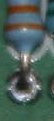
- in one area of the power supply section, on the PCB, there are three components (look like the component in the attached image; I am not sure what they exactly are ) in a row.
- one of these (labeled IC1) measures roughly 3.3V and is flat on the 'scope
- the second one (labeled IC2) measures roughly 5V and shows a 0.2V point-to-point ripple on the 'scope
- the third one (labeled IC3) measures roughly 9V and shows a large 1.4V point-to-point ripple on the 'scope
I take it you mean the section in the attachment.
IC1 is not in the section, did you mean IC12? If so, the 3.3 V is correct. This seems to funcion OK.
But the other two, IC2 and 3, should not have these high voltages. If I read the datasheet correctly the 1587 voltage regulator is either fixed to 1.5 or 3.3 V or, if an adjustable version is used, variable between 1.5 and 3.3 V. This is where I'd start my search for the fault. No surprise, actually, the high ripple already indicated a problem here.
Attachments
jitter said:This is where I'd start my search for the fault. [/B]
Thanks, will do. That is also around where the technician was suspicious due to the ripples. However, we could not tell if it was those specific components (IC2 and IC3) which are the actual problems, or if there is something earlier in the supply section prior to reaching those, that is at fault. Equally perplexing is why it is exhibiting only in the left.
As soon as I hear back from the manufacturer (hopefully they will provide a schematic and not want to keep it secret/proprietary) I'll let you know!
jitter said:Addition: The voltage regs seem to have failed. This in turn might have damaged the circuits they're supplying power to. Better to leave the DAC switched off until the tech has his schematics.
That is worrying
 . The last thing I would want is to find that critical (rather than the cheap, everyday, off-the-shelf) components are faulty. I can imagine that would mean shipping it to Italy to the manufacturer!
The technician gave me a call this afternoon regarding something he thought about after I had left. The L/R channels share a common PSU and all RCA jacks share a common ground. The two lower voltage regulators (3.3V and 5V) are for the digital supply section and the ~9V one is for the analog supply section. He think that the problem may be that the earth on the left channel is incorrect (wired wrong way round) as the PSU is common to both Lt and Rt channels - which is why the hum is coming through only on that channel. I will be taking the DAC to him later this week for test this theory.
What I am not sure of though is how this would come about. The DAC is (according to the distributor) a stock, demo unit with the only changing being the rewiring of the transformers for the voltage change. Would this have possibly resulted in the incorrect earth? Could this exhibit intermittent issues (e.g., worked when the distributor tested in the US using a 115V-->230V converter) but not here?
What I am not sure of though is how this would come about. The DAC is (according to the distributor) a stock, demo unit with the only changing being the rewiring of the transformers for the voltage change. Would this have possibly resulted in the incorrect earth? Could this exhibit intermittent issues (e.g., worked when the distributor tested in the US using a 115V-->230V converter) but not here?
I tried to read the values off of R31-34 and calculate what the output voltages for IC2-3 ought to be, but it seems my color vision isn't good enough. While the ripple on IC3 is worrisome, the 9V (if that's what it's supposed to be) is probably post-regulated by the LF50C4 parts to 5V so the ripple should not get through. I would measure the output voltages of IC7-10 to see how they behave. The ripple on IC2-3 points to either regulator failure, or something upstream (caps, diodes, diode bridges) not working correctly. I do not think this is a grounding issue.
The distributor might've fried or overheated something when the change to 220V was made.
The distributor might've fried or overheated something when the change to 220V was made.
xenithon said:The technician gave me a call this afternoon regarding something he thought about after I had left. The L/R channels share a common PSU and all RCA jacks share a common ground. The two lower voltage regulators (3.3V and 5V) are for the digital supply section and the ~9V one is for the analog supply section. He think that the problem may be that the earth on the left channel is incorrect (wired wrong way round) as the PSU is common to both Lt and Rt channels - which is why the hum is coming through only on that channel. I will be taking the DAC to him later this week for test this theory.
What I am not sure of though is how this would come about. The DAC is (according to the distributor) a stock, demo unit with the only changing being the rewiring of the transformers for the voltage change. Would this have possibly resulted in the incorrect earth? Could this exhibit intermittent issues (e.g., worked when the distributor tested in the US using a 115V-->230V converter) but not here?
Hmm, there's not much wiring in the DAC. Only between the pcb and the connectors and the toroids. Power supply is routed through pcb-traces, so no wiring mistakes are possible there.
Wiring mistakes of the RCA connectors would have been noticed long before you bought it and would not have been intermittent.
Probably the only thing the distributor had to do was connect the primary windings of the toroids in series (for 110 V they're parallel, for 220 V in series) and replace the fuse(s) rated for 220 V.
He would not have needed to touch the rest of the DAC.
If by some mistake he applied 220 V before the rewiring, or made a wiring mistake he may have overloaded something that didn't fail directly. We'll probably never know for sure...
mako1138 said:I tried to read the values off of R31-34 and calculate what the output voltages for IC2-3 ought to be, but it seems my color vision isn't good enough. While the ripple on IC3 is worrisome, the 9V (if that's what it's supposed to be) is probably post-regulated by the LF50C4 parts to 5V so the ripple should not get through. I would measure the output voltages of IC7-10 to see how they behave. The ripple on IC2-3 points to either regulator failure, or something upstream (caps, diodes, diode bridges) not working correctly. I do not think this is a grounding issue.
The distributor might've fried or overheated something when the change to 220V was made.
Same thoughts here...
R31 & R33: gn-br-br-bk (-br)= 511R 1%
R32 & R34: or-or-bk-br (-br)= 3k3 1%
The 3k3 resistors are attached to the ground plane on one side (see attachment). This would mean that they are R2 in the formula from the datasheet:
Vout = Vref (1+ R2/R1)+Iadj(R2)
Vref = typically 1.25 V and Iadj(R2) is so small, it's negligible.
Then Vout = 9.3 V. My assumption the adjustable version of the 1587 can't go above 3.3 V seems wrong.
That's good news actually, that means that the components behind these stabilisers didn't get fried by overvoltage!
If I read the colours correctly, then IC 2 and 3 are set to the same voltage (i.e. 9.3 V), in which case IC2 has seriously low output. This is a power supply for the analogue section. The LF50 behind it probably doesn't get enough voltage to work properly.
Something is going wrong around IC2 which may affect IC3's output as well (without IC3 being defective).
Now it's a matter of finding if the fault lies upstream or downstream (or the stabiliser itself).
Attachments
Hey there and thanks so much for the amazing info. I am going to the technician tomorrow evening and we'll attemp further troubleshooting. Unfortunately other than a brief email from the manufacturer late last week, I have not heard back regarding schematics or possible issues that they suspect.
jitter - your paragraph make a lot of sense
If I read the colours correctly, then IC 2 and 3 are set to the same voltage (i.e. 9.3 V), in which case IC2 has seriously low output. This is a power supply for the analogue section. The LF50 behind it probably doesn't get enough voltage to work properly.
Something is going wrong around IC2 which may affect IC3's output as well (without IC3 being defective).
Now it's a matter of finding if the fault lies upstream or downstream (or the stabiliser itself).
However what I still am perplexed by is why the issue is exhibited in only one channel, when the analog supply is common to both channels and it seems like only one of the stabilizers "services" the analog supply. . Is there anything you suspect that could result in this single-channel issue?
Cheers
X
jitter - your paragraph make a lot of sense
If I read the colours correctly, then IC 2 and 3 are set to the same voltage (i.e. 9.3 V), in which case IC2 has seriously low output. This is a power supply for the analogue section. The LF50 behind it probably doesn't get enough voltage to work properly.
Something is going wrong around IC2 which may affect IC3's output as well (without IC3 being defective).
Now it's a matter of finding if the fault lies upstream or downstream (or the stabiliser itself).
However what I still am perplexed by is why the issue is exhibited in only one channel, when the analog supply is common to both channels and it seems like only one of the stabilizers "services" the analog supply.
. Is there anything you suspect that could result in this single-channel issue?Cheers
X
Agreed, it's strange, but don't forget we don't know what's the cause yet. Judging by your descriptions it has all the signs of PSU failure, but keep in mind something else might be wrong (too).
Besides, you only know the voltages of three of the regulators and there are eleven in total...
Besides, you only know the voltages of three of the regulators and there are eleven in total...
Arrrrrrrrggggggggggggggg!!!!
Ok, now that's off my chest.
The technician spent the past couple of evenings doing a thorough analysis of the various components. Firstly as you may recall, one of the initial findings over the weekend was that the 4 transistors in the left analog output stage seem to have been replaced/changed. This is clearly evident as they had large, uneven solder blobs, whereas every other component on the PCB had very small, uniform, consistent solder. So this was NOT a mint, demo unit, but one on which repair work had taken place. Over and above the uneven solder blobs, there is significant solder flux residue around these components.
These components, labelled J3 and J4, are FETs in the left channel's analog output stage. These were obviously replaced at some stage - either when the voltage change was performed (though I suspect that is highly unlikely as the voltage change would not go anywhere near the analog output stage) or at some point earlier in this DAC's life.
The PCB is double-sided. A replacement of these FET's would require the entire PCB to be removed from the chassis so that they could be properly soldered on, but it is clear that this was not done. Instead, the replacement was only done from the top/exposed side of the PCB (the easy but incorrect and unreliable way). As a result, the contact is problematic and not properly being made, resulting in hum/noise problems in that left channel. The suspicion is that one of the 3 legs of the FET is making improper/inconsistent contact resulting in a ground issue which in turn results in the hum. The contact is inconsistent so it may occassionaly be made and grounded, hence the intermittent nature of the beast.
Irrespective of when the problem with the FETs occurred, the fact remains that an incorrect attempt was made at fixing it and this has resulted in the hum/noise. Properly fixing this requires the entire PCB to be taken out, which involves desoldering all the jacks, LEDs etc. - a time consuming, messy and costly effort (not to mention difficult when this product has never been worked on and without any schematic to assist).
EDIT: for additional info to this thread, those components (J3/J4) were isolated as the problematic ones as the signal was checked on an oscilloscope just prior to going through the FETs and it is clean, but directly after the FETs the signal shows significant ripple, distortion and clipping.
xenithon said:Arrrrrrrrggggggggggggggg!!!!
Ok, now that's off my chest.
The technician spent the past couple of evenings doing a thorough analysis of the various components. Firstly as you may recall, one of the initial findings over the weekend was that the 4 transistors in the left analog output stage seem to have been replaced/changed. This is clearly evident as they had large, uneven solder blobs, whereas every other component on the PCB had very small, uniform, consistent solder. So this was NOT a mint, demo unit, but one on which repair work had taken place. Over and above the uneven solder blobs, there is significant solder flux residue around these components.
These components, labelled J3 and J4, are FETs in the left channel's analog output stage. These were obviously replaced at some stage - either when the voltage change was performed (though I suspect that is highly unlikely as the voltage change would not go anywhere near the analog output stage) or at some point earlier in this DAC's life.
The PCB is double-sided. A replacement of these FET's would require the entire PCB to be removed from the chassis so that they could be properly soldered on, but it is clear that this was not done. Instead, the replacement was only done from the top/exposed side of the PCB (the easy but incorrect and unreliable way).
Not necessarily. I have done many succesful repairs that way on boards that were mounted on big heatsinks with many screws. Double-sided (or multilayer) pcbs have metal plated holes. The only way repair 'from above' will fail is when the plating has been damaged during removal of the component(s). If the damage is not too bad, soldering from both sides will get an acceptable joint.
As a result, the contact is problematic and not properly being made, resulting in hum/noise problems in that left channel. The suspicion is that one of the 3 legs of the FET is making improper/inconsistent contact resulting in a ground issue which in turn results in the hum. The contact is inconsistent so it may occassionaly be made and grounded, hence the intermittent nature of the beast.
If the plating of the holes has been damaged, this is possible. But the repair may also have damaged the FETs themselves. IMHO only one way to find out: removal of the pcb and replacement of the FETs.
Irrespective of when the problem with the FETs occurred, the fact remains that an incorrect attempt was made at fixing it and this has resulted in the hum/noise. Properly fixing this requires the entire PCB to be taken out, which involves desoldering all the jacks, LEDs etc. - a time consuming, messy and costly effort (not to mention difficult when this product has never been worked on and without any schematic to assist).
It may be worth checking if the components on the front side are acually attached to it. Looking at a picture that shows the LEDs and push buttons it seems to me that the pcb can be pulled away without unsoldering them.
EDIT: for additional info to this thread, those components (J3/J4) were isolated as the problematic ones as the signal was checked on an oscilloscope just prior to going through the FETs and it is clean, but directly after the FETs the signal shows significant ripple, distortion and clipping.
And what about the ripple on two of the voltage regulators?
The tech could remove the offending FETs the quick'n'dirty way (from the top) and see if that has any effect on the PSU.
Xenithon, this may be nothing but looking at the pictures of the Analog Supply you can see that R27 and R30 are different resistors, the two caps just below the resistors are different also, I assume that we are looking at L and R channels on the board. Strange that these parts are different in a new piece of gear.
Phill
Phill
- Status
- This old topic is closed. If you want to reopen this topic, contact a moderator using the "Report Post" button.
- Home
- Source & Line
- Digital Line Level
- Assistance in diagnosing Hum/Buzz/Noise