Bricolo said:
Guido,
What is a latch? Is is the instant when the DAC reads the input data (or outputs the analog data)?
And can't reclocking one or 2 of the I2S lines cause problems, since there will be a delay between them?
Thanks
The latch is the internal register that holds the data.
The DAC has a latch that hold the bits clocked in with BCK, loading is done serial, but the internal logic will read the whole 16 bits when WS says the data is there. From there the conversion proces can start.
In the end the output changes: there will be a current during a sampleperiod that reflects the incoming data. This current will be there untill the next sample comes out of the DAC. So also some kind of (analog) latch.
The output changes when the conversion is done (indicated by WS) and on BCK (or SCK with 1541). This is done with the INTERNAL LE signal created by the logic using WS and BCK signals.
In short: the DAC clocks data in on BCK and outputs data on BCK.
So BCK should be jitter/noise free. Best is all three lines.
There are many posts on reclocking. In the datasheet you can find the timingdiagram of I2S and what is allowed an not allowed with timing.
Reclocking all would give the same delay. Reclocking only one is probably not going to hurt if the delay is small. It is allowed in the spec.
mvg,
guido said:Now looking at the logic used.
A standard 4024 is slow, so you need to invert the clock of the '174. Otherwise the '174 would be clocking in and the 4024 hasn't clocked out yet....
delay of the 4024 is 50/60 nSec. 11.2896MHz is 88nSec, so 44nSec between clock high to low and low to high. With the
inverter you get 88nSec+inverter delay for the 4024 to output the data instead of 44nSec which is not enough.
So don't use a superfast 4024, say with a delaytime which matches the inverters delaytime. The 4024 would be clocking out while the '174 is clocking in...And the '174 needs some time that the data needs to be stable before clocking.
Faster logic isn't always better
Or if you use a superfast 4024 you could remove the inverter in the clockline of the '174. The 4024 then has 44nSec minus the '174 setuptime for dataoutput.
Fmax of a 4024 is typical 10MHz at 5V, that is less then 11.2896And minimal is only 5MHz
(looking at philips datasheet of standard CMOS HEF familiy).
Anyone looked at this? Which logic are you using?
Greetings,
According to Henk, a 74HC4024 would fit perfectly
") (as a drop in replacement)
(as a drop in replacement)I've looked at the 74HC74, as a replacement for the 74HC174 (but this way, no I2S line can be reclocked, at least not on the same chip)
This chip leads to a much simplier PCB layout
But I have a few questions:
-since this chip has separate reset and clock inputs, can I simply connect them together (in fact, connecting every input/output of both FFs together) ?
-reset and set have to be connected to Vcc, right? Directly or with a resistor?
-what kind of regulators and decoupling should be used for the logic and transistors?
I'm working on a PCB for it, if someone wants the eagle files I'll share them
Zodiac said:Hi Guido,
Re the logic question...If you use syncronous dividers such as the 74HC163 then delay becomes much less of an issue compared to binary counters like the 4024 / 4040. I am using these without an inverter on the clock line to the flip flop.
Rgds.
Oops, the '163 clock is just the other way around as the 4024.
That's why there is no inverter i guess.
A HC163 has a propagation delay of 17nSec (philips). Mmm.
Check my story, maybe it is too fast ?!! i have to look at this in more detail at a later time. HC4024 is probalbly similar.
No more time for a few days (the girl is flying in and she has a higher interrupt level. It is a non maskable interrupt
I mailed Henk with a question about his implementation and my thoughts, waiting for his reply.
Yeah, i know. Sortof..

Timing, timing...
Guido,
I agree with your calculations about delay time, etc. I am using the Fairchild HC163s, propagation delay Clock to Q is 29ns. These are daisy chained (i.e. one HC163 ripple carry feeds the next HC163 clock), so the total delay is 2*29ns or 58ns.
Using an 11.2896 Mhz clock, 44ns is time between L to H and H to L transitions (i.e. 88ns total cycle time).
This leaves 58ns - 44ns = 14ns for the flip flop. In my case I use the VHC374 which needs 6ns or so (again Fairchild) setup time. That leaves 8ns spare!
I don't have any problems with this, although I have to admit I have not checked it out with a scope as I don't have one.
Rgds.
Re: Timing, timing...
The '163 and '374 are both clock low to high, right? And there is no inverter. That would mean that you have
88 - 58 - 6 = 24 ns spare, right?
Bottomline is that the output of the divider should not happen as the FF is clockin in. It does not matter if the DEM freq is delayed with a few clockpulses. It is not related timingwise to the I2S data clocking in. Only requirement is that it is derived from the same clock.
mvg,
Zodiac said:Guido,
I agree with your calculations about delay time, etc. I am using the Fairchild HC163s, propagation delay Clock to Q is 29ns. These are daisy chained (i.e. one HC163 ripple carry feeds the next HC163 clock), so the total delay is 2*29ns or 58ns.
Using an 11.2896 Mhz clock, 44ns is time between L to H and H to L transitions (i.e. 88ns total cycle time).
This leaves 58ns - 44ns = 14ns for the flip flop. In my case I use the VHC374 which needs 6ns or so (again Fairchild) setup time. That leaves 8ns spare!
I don't have any problems with this, although I have to admit I have not checked it out with a scope as I don't have one.
Rgds.
The '163 and '374 are both clock low to high, right? And there is no inverter. That would mean that you have
88 - 58 - 6 = 24 ns spare, right?
Bottomline is that the output of the divider should not happen as the FF is clockin in. It does not matter if the DEM freq is delayed with a few clockpulses. It is not related timingwise to the I2S data clocking in. Only requirement is that it is derived from the same clock.
mvg,
Bricolo said:I've looked at the 74HC74, as a replacement for the 74HC174 (but this way, no I2S line can be reclocked, at least not on the same chip)
This chip leads to a much simplier PCB layout
But I have a few questions:
-since this chip has separate reset and clock inputs, can I simply connect them together (in fact, connecting every input/output of both FFs together) ?
-reset and set have to be connected to Vcc, right? Directly or with a resistor?
-what kind of regulators and decoupling should be used for the logic and transistors?
I'm working on a PCB for it, if someone wants the eagle files I'll share them
OK Bricolo
For details of how to implement the '74 flip flop, see peufeu.free.fr or the datasheet!
As for decoupling, I would suggest 0.1uf or higher if you can get them ceramics, placed to minimise loop area between Vcc and Gnd.
As for power supply, I am using current sourced TL431s (again see peufeu's excellent site for details). Alternately, I have been experimenting with passive supplies...YMMV. Many logic chips will take 7v, this should theoretically give better results than the nominal 5v. I don't know if it sounds better though.
Rgds
Hi,
Got a reply from Henk that he does not mean HEF logic with '4024'. When i read 4024 i translated that into HEF, my bad!!
HC is fine to use. HEF is too slow.
So for me 74HC4024 or HC161. Have to see how it fits in with the existing stuff (already have one HC161 in use on my dac dividing the 11MHz).
GuidoB
 There's no power supply, and no PS decoupling for the momment.
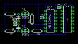
DragonMaster said:Hi, it's the first time I read this topic.
What are 256fs and dem_pin?
Can I use it with normal I2S signals or I need a 4th signal from the CDP if I use it?
Hi,
As I understand it.......
256fs = 256 X 44100 (cd format) = 11289600 Hz
This works out at 11.2896 MHZ so the 256fs is the system clock.
I think this 256fs is divided by IC 4024 (74hct4024) but i'm not sure exactly which divider to use (depends on NON-OS vs OS)
The latch then reclocks the new clock using the original system clock.
Note that WS is also reclocked in the design.
http://www.diyaudio.com/forums/showthread.php?postid=364560#post364560
dem_pin = pin 16, and 17 on the tda1541a (where orignally a cap was)
Kind regards,
Ashley.
DragonMaster said:Ok so I take 256fs from SCLK?
Yes, I saw that WS was reclocked also.
The scheme tells to get the -6v at the 1541A but there's only -5v and -15v.
OK, so the dem pins are the OSC pins finally?
Hi,
SCLK - what IC is it coming from?
I'm not sure about the -6v. I think the bias reistors for the transistors may need to be adjusted.
The dem pins are the osc pins:- I think so..
Regards,
Ashley.
SCLK - what IC is it coming from?
That's the name some people use for BCK. As LRCK is WS.
Anyways, it's not the good one.
I don't know where I'll find a clock of the appropriate bitrate.
- Home
- Source & Line
- Digital Line Level
- TDA1541 DEM reclocking