Ok, I'll give that a go. One thing I'm not good with are things like impedance matching etc. I really found AC theory quite boring at college (ten years ago now), but I wish I'd listened more!
On this PCB though, it doesn't have any ground pins connected on the I2S inputs. This was Nicolas' design (NeoY2k), and the idea was to connect the grounds only at the power supply or something? I know this can be made to work to reduce noise issues and ground loops for analog stuff, but I don't know how to make this work for the digital inputs?
It was Nicolas' intention to design the board this way, I just don't know quite how to hook it up properly, so I'll ask him. The PCB has quite a few RF techniques behind it's design by the looks of it...
eg. In his building guide it says things like "Input connector:
Follow ESS datasheet and schematics. No ground on this connector as it is an input."
You'll notice that the main ground wire in the photo is connected close to the ESS chip. This is also to keep the ground paths short.
The info on this Sabre board is in the following thread for anyone interested (I'll have a read through it again myself)...
http://www.diyaudio.com/forums/digital-line-level/136654-neoy2ks-ess-sabre-dac-platform.html
The thing is, I was also getting the exact same noise issue when using the Buffalo DAC + LCDPS with direct SPDIF input. Although, this was only when using SPDIF from certain sources. This was from either optical OR coax, and from my Audiotrak sound card or certain DVD players. The onboard sound card worked fine however, and all these devices worked perfectly on commercial AV amps?
My guess is that the ESS chip is sensitive to something like differing SPDIF signal offsets as this problem happened before with the Buffalo even via optical, so it can't be a ground loop issue as such?
btw, I know that the comparator opamp on the first version of the Buffalo needed to be changed to lock on to SPDIF signals properly. @pftrvlr - which version of the Buffalo do you have?
OzOnE.
Last edited:
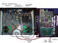
Forgot to mention - in the previous photo, the DAC board is also grounded to the DSP board via the yellow wire next to the ESS chip (same as the main red ground wire.)
The PCB also has a 47K pull-down resistor on each digital input line, and then has a 22 ohm resistor between each input and the ESS chip.
Would it be worth changing any of these resistors to match the impedances better? The inputs are all at 3.3V levels btw.
I realize that this setup is a bit more complicated for fault finding because the DSP adds a lot of variables into the equation, so I appreciate anyone helping with this.
Does anyone remember if the DPLL setting on the Buffalo improved SPDIF lock issues in the past?
OzOnE.
Hi,
I'm glad projects are made using my boards!
However, I don't understand your problem.
You must send a wrong signal, or have incorrect wiring, because the board in itself works - I tested it, and had no crackling noise touching the PCB plane neither.
The grounds are all connected to a single plane, not to independant lines! These lines to ground you find on the "power connector" are meant to sense the real local voltage of the ground plane, at the point it is distributed to the chip, for ie Jung Super Regulators who have both line and ground distant sensing. Or it could be used to ground the voltage regulators, in which case you must NOT provide another ground path for the regulator. It virtually places it as close as possible to the chip.
Oh, I'm a firebreather too. Out of topic xD
80Mhz clock is fine, too.
If I remember correctly too, there are no grounds on the digital input connector!
This is the kind of impedance matching you find in analog: low Z to high Z (47k). No matching! These are meant to be used with short wire. I used 20cm unshielded cable with SPDIF and i2s without any problem! This is the topology used in the ESS demo board too. Strictly speaking, i2s calls for no impedance matching. If you match impedances, you should remove this 47k and the 22R, use 100R and 0R, use 100R at source, but you'll have to output MORE than 3.3V unloaded: 6.6V, so it will remain 3.3V at the inputs and won't shift the decision point.
These were meant to allow you to assing a ground line between each signal line on the multiwire connecting to "digital input". So noise picked up along the line is injected as current at the output stage of the source - so a transformer or active stage takes care of it.
This is another kind of general practice: move noise at outputs, not at inputs.
So ground IS available at the analog outputs, not on the digital inputs.
Tell me more so I can help you.
Cheers")
Nicolas
I'm glad projects are made using my boards!
However, I don't understand your problem.
You must send a wrong signal, or have incorrect wiring, because the board in itself works - I tested it, and had no crackling noise touching the PCB plane neither.
The grounds are all connected to a single plane, not to independant lines! These lines to ground you find on the "power connector" are meant to sense the real local voltage of the ground plane, at the point it is distributed to the chip, for ie Jung Super Regulators who have both line and ground distant sensing. Or it could be used to ground the voltage regulators, in which case you must NOT provide another ground path for the regulator. It virtually places it as close as possible to the chip.
Oh, I'm a firebreather too. Out of topic xD
80Mhz clock is fine, too.
If I remember correctly too, there are no grounds on the digital input connector!
This is the kind of impedance matching you find in analog: low Z to high Z (47k). No matching! These are meant to be used with short wire. I used 20cm unshielded cable with SPDIF and i2s without any problem! This is the topology used in the ESS demo board too. Strictly speaking, i2s calls for no impedance matching. If you match impedances, you should remove this 47k and the 22R, use 100R and 0R, use 100R at source, but you'll have to output MORE than 3.3V unloaded: 6.6V, so it will remain 3.3V at the inputs and won't shift the decision point.
These were meant to allow you to assing a ground line between each signal line on the multiwire connecting to "digital input". So noise picked up along the line is injected as current at the output stage of the source - so a transformer or active stage takes care of it.
This is another kind of general practice: move noise at outputs, not at inputs.
So ground IS available at the analog outputs, not on the digital inputs.
Tell me more so I can help you.
Cheers
Nicolas
Hi, Nicolas. How's it going?
Sorry I didn't get around to e-mailing you yet.
Again, my usual apologies for quite a long post. I'm hoping at least a few people might enjoy reading this just for the sake of it (I know I enjoy longer posts occasionally).
I'm certain the board is working fine and it's very well designed, but my problem is simply down to the way I've wired everything together...
I no longer get the crackling when touching the board etc. since I improved the power supplies and wiring and also fitted a mains filter.
What I have now noticed though is that my grounding point (for the mains filter) is not making proper contact with the whole amp chassis - if I push down on the bottom panel of the case, I hear a pop from the speakers, and the DAC resets itself (probably more like a data glitch, since the reset line now is tied to directly to ground.) So, I'll have to sort this out since I'm sure it's contributing hugely to the issue.
I realize that a lot of the design of the PCB is for remote sensing etc. I have the shield connected to ground at the moment (two points connected).
The 80MHz clock appears to be working great now as the quality is excellent. I'm still getting the strange noise at the start of decoding though, and it would suggest a problem with the DSP, although as I say, the noise I'm getting is the same as I remember getting with the Buffalo (with certain sources). It "sounds" like an async PLL is trying to lock on, but this is just a guess of course.
So, I have to sort out the grounding issue first, and try a ground lift and different wiring topologies for the power supplies.
OK, one big clue is that I'm actually using a +5V SMPS to power the DSP board, so this could cause big problems. The CPU is powered by a small standby transformer, the amp modules are powered by a 300VA Nuvotem, and the DAC board is powered by the TP LCDPS (all 1.2V and all 3.3V lines connected together.)
I need to build a quick +5V PSU for the DAC board and do away with the cheapo SMPS as I'm sure this will improve things a lot.
Another thing which happens is that if I try connecting my Sure 4*100 Watt amp module to the DAC board, it of course sounds very distorted because it needs at least a simple buffer or I/V stage by the sound of it. The thing is, I also get a buzzing sound while the DAC is in mute and this sounds very much like the typical ground loop "noise" you get with SMPS'.
Should I try connecting every power supply minus together, and then try connecting to the mains earth? What would be the recommended method?
btw, I have now changed all the digital inputs to use short lengths of mini-coax. The BCLK and LRCLK connections are each only 3 cm long, and the DATA input connections are only 5 cm long. The shields are currently grounded at the DSP end, and connected to each other at the DAC end....
Should I still ground the coax shields at the DAC end as well? I'm not sure what to do with the resistors in this case?
Thanks,
OzOnE.
Star ground doesn't work for digital.
Analog signals don't need impedance matching because the wavelength is measured in miles. In digital, the switching edge of a I2S pulse is nanoseconds, with a wavelength in inches. This absolutely needs impedance matching to preserve the waveshape of the logic pulse.
The geometry of twisted pairs or coax is specifically designed to keep the return current of the signal close to the forward current. This way the magnetic fields cancel since the currents and their magnetic fields directly oppose.
Cancelling magnetic fields is critical when your wavelength is inches. By grounding at only one end, you force the return current to take a big circle path back to the source. You have a huge ground loop as seen by a 100MHz digital logic pulse. You are broadcasting digital noise.
Ground the digital cables at both ends.
You know what, I've never had ground loops explained in that way before. Makes a lot of sense to me. Basically, it's like producing a loop antenna is it not? I should know better really, I spent a fair amount of time reading Tesla type RF stuff in the past.
I've grounded both ends of the coax now, so it should be fine.
(I just wanted to say that Nicolas' PCB design is very well thought-out and it's only my naivety which led to the more basic questions.)
I'm sure the I2S connection is fine now, but I still get the noise when the source changes track etc. I have to admit, it could possibly be the DSP board after all. I know my setup is a bit of a mismash of parts, so it's probably down to the SMPS on the DSP or something.
I've sorted the eathing problem now and it has good contact through all of the chassis (mostly aluminium I think). I have no intention of leaving the mains earth disconnected obviously.
What I realized yesterday was that the DAC board is actually grounded via the Sympatico modules! This of course goes to the center-tap of the big torroid, and all other grounds are insulated from the case (mains earth) - If I'm not getting any major noise issues now, is there any reason to ground the center tap of the trafo to mains earth, or can it be left floating?
(I should really draw out a rough diagram of the connections today. I might also take a recording of the digital noise I'm getting.)
btw, the original DAC on the Denon used mute transistors on each output... The Sabre DAC is only using the auto mute function atm. It is fairly slow to come out of mute (with the register defaults), but the noise still continues for about half a second after the Sabre un-mutes?
I'm confident that there's no way the original muting lasted longer than this noise (ie. to cover up any DSP setup noise etc.), as the Denon was almost instant at locking onto new signals before.
I'm even using the PC as a source via coax now, and the short burst of noise sounds exactly the same?
Apart from this small issue though, everything else is working great.
Thanks again,
OzOnE.
Here is a recording of the noise I'm getting. Please ignore the background noise, it's only the PC fan etc...
Digital Noise (OzOnE amp).wav
This was from the first few seconds of Black Hawk Down (DTS). The noise is the same whether the source is PCM, DD, DTS. After this noise, playback is then perfect (it only happens when the Sabre first comes out of mute).
Again, granted, it could well be the DSP itself or the digital receiver. It sounds like a PLL is out of lock and it's just hunting to find the correct phase of the incoming signal. Although, as it happens with PCM and compressed formats, it's unlikely to be a digital receiver problem as I'm sure it would create an entirely different sound (I would expect signal corruption on lossy formats to cause a much nastier sound.)
I don't want to take up too much of anyone's time on this subject, so I'll concentrate on building the rest of the amp now and figure this out at a later date. However: has anyone heard this sort of sound before?
Regards,
OzOnE.
Hello,
Yes - you should make a clear drawing of your wiring!
I don't fully understand it just with words...
Regarding the CT/Mains earth, common practice is:
CT directly to the midpoint between the two filter capacitors (shortest possible).
Then a wire from CT to chassis.
Then a wire from Mains Earth to your CT/Chassis connection, at the chassis bolt.
Ground every "signal ground" at the CT point where it connects to capacitors.
If you have many connection, make a bus bar or star ground with anything thick and highly conductive (ie copper bar).
If you want to, ground "shields" to chassis locally, do NOT travel the unit to join the earth bolt. Other solution is: ground "shields" to the "signal groundplane" locally (that's why I provided this connection option on board).
If you want to go further, you can consider filtering between these shield connections and the chassis or ground, but I leave it to you.
You may use "ground breakers" etc... But first make sure you can safely power your equipment.
It seems you have some ground loops problems anyway. Show me a drawing.
Regarding the "star grounding doesn't work for digital"... yes and no: better a star ground than a bad "short loop".
Oh damn... It's gonna be a long post. I'll try to make it clear, but I already know it won't be clear...
Imagine you'd like to have a big solid ground plane, cause that's what works for RF. Then deal with solutions in the real world.
IE: if you look closely at the board, you'll see that 100nF caps run exactly under the power trace to each pin. This way, you cancel most EMI and do not radiate it over the case/board. But it also increased Z and L of ground connection by the use of a via, so it reduced bypassing efficiency globally and modified ringing frequency (put it lower). The loop is ultra small in lenght, but don't forget it has some height and that the ground plane in between will absorb part of these radiated currents at a place you just wanted them to directly cancel. If I just put these caps on the top, it would have meant a longer loop, and there wouldn't have been any cancelation. Which one is better? Hard to know. No free lunch. I thought the "bottom" option was better but I couldn't compare.
Why am I saying all this? Because you have to make loops short, but loops are not just defined by their lenght, but also their impedance and some other factors.
If you allow a small loop for say i2s return currents, that's in itself a good idea. Fast signals want to see small loops. But if you are injecting lots of other trash currents in it, and/or it isn't really low Z, wouldn't it be better to make these currents take another path, maybe a bit longer - but not developping a noise voltage right at the input pins!? i2s is not Ghz, just a few Mhz - you want it clean, ok, but relax!
Your DSP board has a connection to ground.
Your DAC board has a connection to ground.
But how well are these grounds connected?
It seems they don't even use the same supply, one is SMPS the other one linear... You have to directly connect the SMPS ground to the center tap of the linear one. And you know you are injecting some serious spurious currents here! That's why you need a short solid connection, otherwise it will develop as noise voltage.
If you rely on chassis, or worst, on your i2s "return current" lines to handle these spurious currents, it is normal the system has some serious problems!
If you imagine a virtual groundplane, you'd like to connect the i2s line AND ground lines directly between the boards. In fact, you wouldn't even need a seperate ground connection for the DAC board or the DSP board.
If you imagine a star ground, you don't want this i2s return currents connection as it makes an extra loop.
The faster the signals, the closer to the signal trace flow the return currents on the ground plane.
So yes, you would like to connect the grounds between the two boards with the i2s connection, so these noise currents wouldn't radiate.
This loop has it pros and cons: it provides a short return parth for i2s line currents. This is good. But if the main ground connection to ground of each board doesn't results in a low Z between the ground found on each boards, you are injecting ground currents right at the input connector, and allowing them to develop voltage on this connector (these are holes, and wires, so L and Z!).
So, connect or not connect? Take it with a big grain of salt: CMOS inputs are not that sensitive, and i2s lines do not generate really big currents.
The ground connection of the whole board is very close to this input connector, this is not just pure luck, you can have some serious low Z connection here. Now, you might as well not have this loop, use a star ground. It will probably work as well.
All that to demonstrate what? That the problem in your system is probably not here xD but more on this interconnection between the several grounds of your boards (the SMPS ground to CT stuff etc).
For the digital inputs connector, I don't see why you would do impedance matching??????? Hey, it is CMOS logic, it has no impedance matching, nor is it meant to be used with twisted pair or impedance controlled traces!
There is no impedance matching for the clock neither, this is low output Z to high input Z connection, just like LF analog!
The Buffalo board nor the demo board do provide any impedance matching on their i2s input lines!
You might not like it, and you'd be right: nearly all recent FPGA have LVDS inputs and outputs, to handle fast signals cleanly, not only on long distances, but also on short ones.
This is not the case here. If you want to do impedance matching, you have to get twice the output voltage as the final desired voltage. Your signal is expected to be CMOS level, so you'd need twice the CMOS level at output.
This is not the case, you may do it for you but this wouldn't be i2s anymore, strictly speaking.
You don't even need coax to connect i2s lines between the boards. You're not in an impedance controlled environment. You may connect the cable shields to chassis "shield" connections.
OK, that was a talk for the pleasure of technical illness.
What is WAY MORE of a problem is that you connected these "ground sense" lines together on the power connector, as far as I understand?
This is NOT what you should do! There is a ground plane to do it! Doubling it makes for big loops through the dedicated traces!
You connected them to the regulators (LCDPS), and these are themselves grounded through a dedicated wire?
NO: you have to choose, or you locally ground them, or you ground them to the star point, not both. And as you don't have 7 independant regulators, local grounding makes no sense, you're making big loops.
Cut that ground connection between regulators and the board: it is already done via the star point.
Once THAT solved, and the SMPS ground to center tap ground problem solved, you shouldn't have this problem anymore.
Or it would mean that it is related to something else like incorrect signal timing or who knows. A bad ground connection may not be a disaster on the DAC board, but may throw the DSP board's PLL out of loop.
I hope it will help you.
Cheers,
Nicolas
For the digital inputs connector, I don't see why you would do impedance matching??????? Hey, it is CMOS logic, it has no impedance matching, nor is it meant to be used with twisted pair or impedance controlled traces!
There is no impedance matching for the clock neither, this is low output Z to high input Z connection, just like LF analog!
you are wrong
I'm not going to argue with you.
google something like:
return path impedance control digital
and read some articles.
Howard Johnson's book "High Speed Digital Design" is very good. you should read it.
The Buffalo board nor the demo board do provide any impedance matching on their i2s input lines!
They have grounds on the connectors for the return currents ! They also have 22 ohm series termination resistors on the inputs to damp reflections.
Thank you, but I know about return path etc.
I already have some RF books, but howard johnson's is on my wishlist, you're right.
CMOS inputs are high impedance, that's all! On my board (as well as yours, as well as ESS's, so don't get me wrong on this "cmos input impedance" thing), there is a pull down resistor (if I remember correctly, 47k), and a serial resistor.
There is a difference between 22R (that I have too) to damp reflections and limit current and a real "termination".
What I would have called termination would have been ie: he used 50R coax, so he used a 50R source and a 50R termination too ground.
Or a twisted pair, so he would have used 100R source and 100R termination. Hence my recommendation that he sets the right resistor values in the case he wants to do so.
BUT this termination will eat half the voltage, so he would need to output his signal at a 6v6 level to keep the decision point at half the waveform.
Now, as I said in my previous post, closing this loop here "If you allow a small loop for say i2s return currents, that's in itself a good idea" is a good idea in most cases.
What's important is the current; because YES you want to provide a return path for the i2s lines, but if you inject a lot of spurious currents via this connection, you'd be better off another way.
And that was the case I had in mind (computer source), where I feared injecting more spurious via this connection, than avoiding by providing the shortest path for the i2s lines.
And "The ground connection of the whole board is very close to this input connector, this is not just pure luck, you can have some serious low Z connection here."
So in your case, you need it, you directly have acces to the center ground point of the board. At 1cm of the input connector (approx).
I didn't connected the grounds on the input connector because I could easily have both solutions that way: connect ground to the big ground point, or do not connect it without having to cut one of two wires on a flat cable - something that could have been really boring.
Now I realize that for most users, this isn't the best solution. But I first made the board for myself, then sold some, and this board should have been part of a setup of boards. And, anyway, this is not a big problem, the ground point is 1cm away!
Regarding i2s, I tested it with up to 40cm cable, unshielded, and no direct ground connection. It worked without any major problem nor excessive audible jitter. Yes, a real termination would be better here (didn't I said that also in my previous post?). But a simple wire will also work. Now, find your compromise between the two.
Note about the ESS losing sync: I had this on a crappy computer (in fact, the one I'm typing on right now...) that messed a lot with the soundcard synchro and occasionally created "clics". Default jitter bandwith is very low, and may be too low with some systems. Also, remember it is really lower on the ESS9018 than on ESS 9008, so if it was barely working with the 9008 (working with spdif, not i2s) chances are it will have sync problems on the newer one.
Last edited:
i2s is not Ghz, just a few Mhz - you want it clean, ok, but relax!
This is a common misconception. The I2S signals are square waves, not sine waves.
at 44100, the clock is 2.8MHz and the word clock is 44100 Hertz. But the edge of the square wave is fast. Let's say the low-to-high is 2 nanoseconds. That means the clock line has a 2 nS low-to-high, then 175 nS of stable 3v3, then 2 nS of high-to-low, then 175 nS of stable 0v.... repeat...
2ns high-to-low plus 2nS low-to-high = energy with a 4 nS period. 250MHz.
it is the edge rate that matters, not the clock period. The 44100Hz word clock has that 250MHz energy when it changes state.
You need to arrange for 250MHz signal integrity on your I2S lines to keep the correct shape of those clock edges and to get them to the CMOS input at the right time.
CMOS inputs are high impedance, that's all! On my board (as well as yours, as well as ESS's, so don't get me wrong on this "cmos input impedance" thing), there is a pull down resistor (if I remember correctly, 47k), and a serial resistor.
I am not commenting on the impedance of the input. I'm commenting on the impedance of the transmission line and the signal integrity of the data and clock.
What's important is the current; because YES you want to provide a return path for the i2s lines, but if you inject a lot of spurious currents via this connection, you'd be better off another way.
Even better is to ground the I2S lines at both ends and design your system so that you have no spurious currents in those return paths.
Yep. I didn't said it had no importance, otherwise I wouldn't have an SPDIF input circuit I designed sitting in my desk... That has 500Mhz bandwith and shows linear behaviour from the source viewpoint. But 2ns... Many comparators already advertised as "fast comparators" are 7nz... That isn't that fast. Of course, designing for the worst case is clever.This is a common misconception. The I2S signals are square waves, not sine waves.
at 44100, the clock is 2.8MHz and the word clock is 44100 Hertz. But the edge of the square wave is fast. Let's say the low-to-high is 2 nanoseconds. That means the clock line has a 2 nS low-to-high, then 175 nS of stable 3v3, then 2 nS of high-to-low, then 175 nS of stable 0v.... repeat...
2ns high-to-low plus 2nS low-to-high = energy with a 4 nS period. 250MHz.
it is the edge rate that matters, not the clock period. The 44100Hz word clock has that 250MHz energy when it changes state.
You need to arrange for 250MHz signal integrity on your I2S lines to keep the correct shape of those clock edges and to get them to the CMOS input at the right time.
I am not commenting on the impedance of the input. I'm commenting on the impedance of the transmission line and the signal integrity of the data and clock.
Yep again, just i2s on headers with a "series termination" on load (it should be on source) is not really a controlled impedance environment - you don't even know the impedance of the transmission line as it depends on what cable will be plugged in.
My point was that for very short distances, any wire would do the trick. I know this is not the best solution, but it still works in practice.
A few cm of wire shouldn't cause a loss of lock. Now, from the jitter point of view, it is of course worse than a perfectly controlled environment.
Ok, I dug a document from my hard drive for Ozone: read AN-610 from Fairchild, chapter "series termination". You'll see that you'll have to replace that 22R by a shunt, use a coax line (and in that case, I admit cutting the ground on the input and having to connect it a bit further is not the best), compute the Zs, and put that resistor at the source. That way, it will be done correctly if you want "series termination" on i2s lines. And yes, it will be better than just flying wires.
I considered it was low to high impedance matching, because it still is, with some damping, as I couldn't really call impedance matching a resistor to mach an impedance you don't even know, that's all.
Even better is to ground the I2S lines at both ends and design your system so that you have no spurious currents in those return paths.
This was a board for prototyping... I don't even use it now, though it works and was tested in the studio.
I wanted to provide so many options that it became a bit complex to explain wiring in the end...
But now that I look at it and there is someone using this board on his own system, I see the decision to cut the gnd from the connector was rather lame, cutting it on the cable if needed would have been better.
Well, a ground pin is very close, and bonus, it is the main ground of the board, so it isn't that hard to connect.
Last edited:
Hi, guys,
Wow, amazing how fast these discussions can change! I have quite a lot of catching up to do.
Maybe I should have explained from the start that Nicolas' board was designed to be connected in a specific way, but I didn't / don't have full understanding of the techniques involved. I also should have remembered that it was designed to be connected directly to the source via fairly short wires etc.
I didn't intend to start any heated discussions with my questions, but hopefully we all understand that different design methodologies are employed here. As long as we're all learning things, then it's all good I suppose (hell, this is what the forum is for isn't it?)
Anywho, I've drawn up a quick diagram of my current test setup. Again, it's not pretty and I'm sure my earthing point could be a lot better. I also need to earth every panel of the chassis more securely.
The CPU ground is of course connected to the DSP board ground at the DSP board itself, the LCDPS ground are connected together at the LCDPS itself. The DAC board's central ground is connected to the LCDPS, but also via the Sympatico module input grounds, and then through the big trafo CT to mains earth.
Then there is the SMPS for the DSP which I still need to get rid of as I'm sure there are some unwanted current peaks and noise looping around here.
The I2S coax is ground at the DSP end, and also at the DAC end (although it is connected to the "other" ground point atm, not to the one directly next to the ESS chip).
It's still working fine apart from the noise at the start of decoding. I will sort this out once I get my o'scope back and when my buspirate arrives (to analyse the original mute logic timing and to control the DSP directly etc.)
I think it's best for me to leave this subject for a while after this, as everyone's been so helpful already and I've taken up a lot of time in this thread. I will post more updates when I get some of the bigger build issues done.
I just wondered if there's any major no-no's that jump out from looking at the attached photo?
I'll probably start a new thread about the controller side of things when I decide on which CPU board I'm going to use. I'm currently looking at a nice ARM9 board with a 3.5" touch-screen LCD which I'll build into the front of the chassis (these boards can be bought VERY cheaply from China now).
I can then add MANY different upgrades as a go along. It would be fairly easy to add analog inputs for example - I'm using the Sabre for volume control though, but I have no problem with adding a nice ADC and passing analog audio via the DSP and Sabre for speaker delays and bass management (ie. no "direct" mode).
I still have two DSP kits as well (Analog Devices and TI), so I might be able to add some extra goodies to the amp. Although, I do want the controller to be kept fairly simple, but with some nice menus and simple source code.
Just look at what can be achieved with a simple 12MHz AVR chip! (not my video unfortunately)...
YouTube - Homebrew device with iPhone aspirations
Anyway, I'm getting quite off-topic again.
OzOnE.
352.8 kHz / 24 bit I2S input
My project partner, Chiaki succeeded in playing 352.8 kHz / 24 bit DXD audio files by connecting ESS 9018 2 CH Evaluation Board to his SDHC Memory Card Transport (Its name is "SDTrans192") via I2S interface.
http://www.diyaudio.com/forums/digi...ory-card-transport-project-9.html#post2016617
As of now, his success is limited on "No Over Sampling Mode" because the normal evaluation board can not provide a clock frequency high enough for 352.8 kHz fs. After replacing the original 40.0 MHz clock crystal with 80.0 MHz one, he will try a 8 x Over Sampling mode. Have you ever try this?
Bunpei
Chiaki could confirm a play of 352.8 kHz / 24 bit I2S signal input on normal 8 x Over Sampling mode by injecting an external processor clock of 22.5792 x 4 MHz to ES9018 chip.As of now, his success is limited on "No Over Sampling Mode" because the normal evaluation board can not provide a clock frequency high enough for 352.8 kHz fs. After replacing the original 40.0 MHz clock crystal with 80.0 MHz one, he will try a 8 x Over Sampling mode.
http://www.diyaudio.com/forums/digi...ry-card-transport-project-10.html#post2018495
Bunpei
Damn great! Good performance!
It would be cool to know what format Pyramix workstations use for DXD.
Even though DXD is kind of a marketing hoax... Surf on the DSD vague by naming a PCM coding "DXD"... Pray noone will think twice about it... :/
Half Out topic rant:
It would be cool to know what format Pyramix workstations use for DXD.
Even though DXD is kind of a marketing hoax... Surf on the DSD vague by naming a PCM coding "DXD"... Pray noone will think twice about it... :/
Half Out topic rant:
Rant about merging: their worksations are just the cheapest computers (low end motherboard, low end consumer grade parts... No Tyan/Supermicro, no RAID, plain basic cooling/PS...) sold for 4000$ + 4000$ for the DSP. That wouldn't be so much of a problem if it didn't crashed... Well, everyday.
Selling crap to pros who need reliability... Doesn't makes me want to trust you. Business is business, yeah, I know.
About audio "business is business": To the Big Name who'll probably read my messages, waiting for me to put him publicly in flames: it's sad you don't even show respect to your associates. I won't put you in flames, I have more respect than you do, but dare to come back and you'll hear some high level street litterature xDEnd of rant xD
There's the "TG Link" I can remember as of a "private standard" to transmit i2s. There's DCS i2s link too. There was an Onkyo PCI soundcard too, if I can remember? And these Musiland USB/I2S-SPDIF converters (told them to use 75R BNC, not 50R, did they changed it?) use their own on too.
If they all would be level-compatible, a big MUX or router could care for all formats, but they are not - now, maybe CMOS level into LVDS receiver saturates the logic but keeps it "glued" short enough to still transmit the signal correctly... Then you could make an universal input in logic. Some tracks to play with if you want
These would allow DXD streaming from computer. But, appart from Merging, does any software uses it?
You see beautifull TIM on merging's ads, but:
1- Does your hearing goes to 150kHz?
2- Does any opamp settles to the said 32 bits precision in the sampling period? (the AD797 can't...)
Last edited:
I'm quite a layman in your pro world where Merging Pyramix or DAD AX24 or ProTools dominates. Both Chiaki and I are inhabitants of PC-Audio world. So my understanding might be incorrect.It would be cool to know what format Pyramix workstations use for DXD.
Even though DXD is kind of a marketing hoax... Surf on the DSD vague by naming a PCM coding "DXD"... Pray noone will think twice about it... :/
We just downloaded "DXD" files available on 2L Hires Web site. Those files are the only DXD files we have ever known. Before we decided to challenge DXD files, we knew nothing about it. However, once we downloaded the DXD file, we found its file extention was "WAV". We could dumped and hacked its WAV header part. (For example, such audio editor as "Wavosaur" (Wavosaur free audio editor with VST and ASIO support) can read and edit those "DXD" files without any problem.) We are not sure whether those "DXD" files on 2L Hires Web site are of genuine "DXD" file format or not. Anyway, we treated those files as simple PCM Integer 24 bit format though its sampling rate is 352.8 kHz.
I think your questions are really sharpshooting. However, hi-res seems to have a potential for better sound quality for me. I don't like 5 kHz wave shape is represented only 8 points in 44.1 kHz fs.You see beautifull TIM on merging's ads, but:
1- Does your hearing goes to 150kHz?
2- Does any opamp settles to the said 32 bits precision in the sampling period?
Bunpei
1- Does your hearing goes to 150kHz?
2- Does any opamp settles to the said 32 bits precision in the sampling period?
Dear NeoY2k,
Yesterday, I could listened to the sound of some 2L DXD files ( 352.8 kHz / 24 bit PCM format ) for the first time using Chiaki's SDTrans192 and ESS Technology ES9018 2 CH Evaluation Board with 100 MHz oscillator for processor clock.
I think I could detect a fine structure even among faint string vibrations in contrast to its 96 kHz version when we played 352.8 kHz version of Hydn String Quartet. It's truely an amazing experience for me. I believe it's not due to any pracebo effect.
The ES9018 chip is an amazing product.
Bunpei
- Home
- Source & Line
- Digital Line Level
- ESS Sabre Reference DAC (8-channel)