Hi I have a question for you guys. Bypassing op-amps with low ESR caps should be trivial, but not for me") In attached image we have three situations or actually two (because B and C are almost identical). But if you carefully look at picture A) you can see that power supply rail first meet bypass cap, which should in theory lower ripples. After ripples are damped current reaches op-amp. Different thing happens in B and C. Here AC ripples which are generated in power supply rail reaches op-amps -V pin and I don't know what the hell happens next. Could you please explain me is there a difference between these pictures?
In attached image we have three situations or actually two (because B and C are almost identical). But if you carefully look at picture A) you can see that power supply rail first meet bypass cap, which should in theory lower ripples. After ripples are damped current reaches op-amp. Different thing happens in B and C. Here AC ripples which are generated in power supply rail reaches op-amps -V pin and I don't know what the hell happens next. Could you please explain me is there a difference between these pictures?
In attached image we have three situations or actually two (because B and C are almost identical). But if you carefully look at picture A) you can see that power supply rail first meet bypass cap, which should in theory lower ripples. After ripples are damped current reaches op-amp. Different thing happens in B and C. Here AC ripples which are generated in power supply rail reaches op-amps -V pin and I don't know what the hell happens next. Could you please explain me is there a difference between these pictures?Attachments
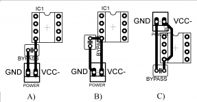
1st the cap, then the pin of opamp.
If you use sockets, you can put the caps under the PCB/under the opamp, as here:
http://s3t.it/data/uploads/axo3assembledbottom.jpg
but i doubt the electrolytics i've used do anything at all - small electrolytics are not recommended by me
If you use sockets, you can put the caps under the PCB/under the opamp, as here:
http://s3t.it/data/uploads/axo3assembledbottom.jpg
but i doubt the electrolytics i've used do anything at all - small electrolytics are not recommended by me
Because traces have resistance, even though small, you always want to hit the bypass cap first, and then go from there to the device. Same as with big filter caps- no ac or noise on the same wires as useful power or signal.
I tend to bypass my opamps with small radial film caps, usually a 0.1 uF Mylar, but there are lots of choices and arguments for different types. There should also be a reservoir cap of 100 uF or so nearby or at least on the same board.
I tend to bypass my opamps with small radial film caps, usually a 0.1 uF Mylar, but there are lots of choices and arguments for different types. There should also be a reservoir cap of 100 uF or so nearby or at least on the same board.
Inductance is to be avoided at all costs when decoupling, so the smaller the cap package the better, and the smaller the leads and traces between the capacitor and the devices power pins the better. The best caps for decoupling close to the pins are usually X7R MLCC SMD devices, small footprints available and low parasitic inductance.
If you are doing your own boards the best results for low level signaling are power ground plane pairs, the added planar capacitance helps decoupling and they provide a much lower inductance than traces.
If you are doing your own boards the best results for low level signaling are power ground plane pairs, the added planar capacitance helps decoupling and they provide a much lower inductance than traces.
You have not shown the ground connections. Taking a point on a PCB and calling it GND does not make it ground; even worse if there are two points called GND. Also, are these RF bypasses or audio bypasses? Is the chip the source or victim of interference? Is ground bounce an issue in this application?
http://sites.ieee.org/ctx-emcs/files/2010/09/Archambeault-Ground-Myth.pdf
Page 37 is one favorites.
Personally I prefer return or ret as a name for what is our PCB's arbitoray 0V point.
My view is that if you live in any civillised part of the world these days then you are going to be awash with RF, so employing basic RF decoupling on the PCB is best practice. A range of cap values will cover all options with a very small low value COG MLCC SMD cap between the pins for RF, with some higher values to provide broad band decoupling and to help lower the power delivery systems overall impedance.
The return plane is a vibrant thinbg, very rarely being atone voltage as DF as said, but depending on the current drawn by the circuitry connected to it at numerous different voltages (Delta I noise) or ground bounce. Decoupling be it for digital or analogue is about controlling this, and making sure any variations are at levels that dont affect your signal integrity.
Yep, got a fair few notes from Dr Bruce, he does a lot of good stuff, mainly for signal integrity and power systems. Well worth a read along with Henry Ott for views on providing the best return paths for any signals and thus improving the integrity of said signals, again for both analogue and digital.
- Status
- This old topic is closed. If you want to reopen this topic, contact a moderator using the "Report Post" button.
- Home
- Design & Build
- Construction Tips
- Bypass caps in pcb