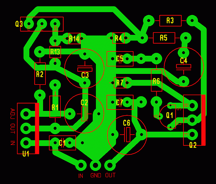
Did some attempts to create my own layouts before, it has always been a pain in the a** for me. Today I gave it another try 
First I'd just like to know if I built in some (seroius) flaws or if my way of thinking is alright so far. In addition I'd be happy to get some links to some tutorials ASO. I guess there is another fundamental than just trial 'n error ...
First I'd just like to know if I built in some (seroius) flaws or if my way of thinking is alright so far. In addition I'd be happy to get some links to some tutorials ASO. I guess there is another fundamental than just trial 'n error ...
When you say a flaw, do you mean an actual electrical error, rather than simply a less-than-elegant component placement etc.? These days I use a schematic capture and layout package that generates a netlist, ensuring that I don't make an electrical error in the placement. In fact, it won't even let me make an erroneous connection when laying out the board. Once complete I can run a Design Rule Check (DRC) and check for errors such as tracks too close together etc.
The one I use is Kicad - it's free.
The one I use is Kicad - it's free.
When you say a flaw, do you mean an actual electrical error, rather than simply a less-than-elegant component placement etc.?
Indeed I meant errors, thanks for clearing things up. I've just downloaded KiCAD, will try it tonight.
Assuming it is correct electrically, your layout looks fine to me, with everything placed around a low impedance ground. But in a circuit like this, I wonder if there would be any reason not to flood fill everything with ground to make it even lower impedance? (Easy to do with packages like Kicad).
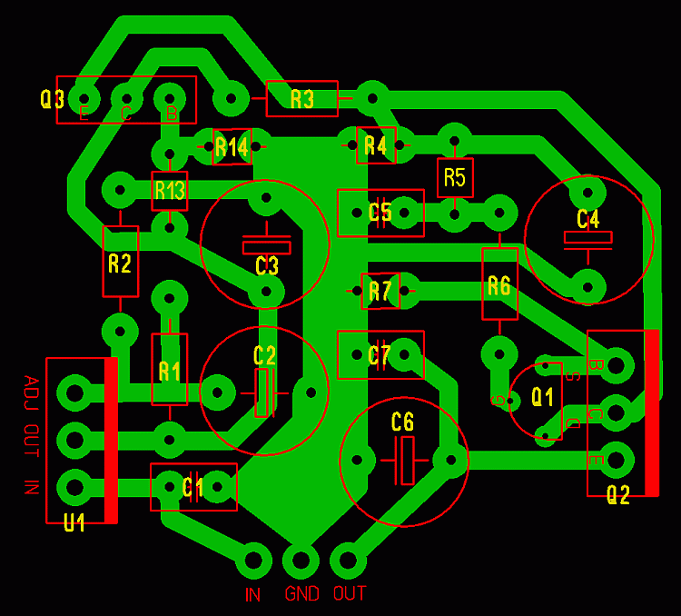
Being the cautious type, I might swap U1 around so that I could, if necessary, bend the chip down and bolt it down for heatsinking purposes if I later found it necessary.
Don't forget your PCB mounting holes.
Being the cautious type, I might swap U1 around so that I could, if necessary, bend the chip down and bolt it down for heatsinking purposes if I later found it necessary.
Don't forget your PCB mounting holes.
Indeed I meant errors, thanks for clearing things up. I've just downloaded KiCAD, will try it tonight.
Good luck!
I asume that red is your silkscreen layer. I would put all the parts numbers (yellow) on the silkscreen layer in such a way that when the components are in place the part# is still visible. Add polarity info to the electrolytics. Your R4, 5, 7 13 and 14 seem to be "standing up" you have enough space on your board to lay them down. Good board for a first try! E
Hi everyone. This seems like just the thread for me, as I was going to come and ask advice in getting every bit of sonic performance out of my boards.
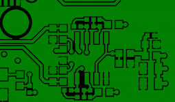
I've laid out this PCM2706-based really simple USB DAC and I'd like your opinion on the board. Does it look ok? The bottom side is all continuous copper. I have little experience in dealing with analog signals on PCB since I'm a more digital guy. It would be especially interesting to hear about what kind of capacitors to use or not to use, where to put them and so on. I don't want to lose any sonic performance because of bad PCB design.
I don't have a schematic to post right now but will post that later today.
I've laid out this PCM2706-based really simple USB DAC and I'd like your opinion on the board. Does it look ok? The bottom side is all continuous copper. I have little experience in dealing with analog signals on PCB since I'm a more digital guy. It would be especially interesting to hear about what kind of capacitors to use or not to use, where to put them and so on. I don't want to lose any sonic performance because of bad PCB design.
An externally hosted image should be here but it was not working when we last tested it.
I don't have a schematic to post right now but will post that later today.
Firstly, the PQFN requires more vias down to ground, preferably 1 per ground pin.
Whare are the power tracks!
This is digital mainly, each ground pin should be viaed down to the ground plane, not routed to star points.
Move the capacitrs on the crystal to the otherside of the crystal and minimise the track length.
Put a ground guard ring around the crystal signals.
Turn C22 around.
where are the decoupling capacitors!
In post #8 I put a text document with some basic PCB design related links, all are relevent to PCB design.
Some relevant to mixed signal design.
http://www.hottconsultants.com/techt...gnd-plane.html
http://www.elmac.co.uk/pdfs/Lord_of_the_board.pdf
An intuitive, practical approach to mixed-signal grounding
http://focus.ti.com/lit/an/sbaa052/sbaa052.pdf
http://focus.ti.com/lit/ml/slyp167/slyp167.pdf
http://www.ieee.org.uk/docs/emc1206a.pdf
http://www.icd.com.au/articles/Split...s_AN2010_6.pdf
http://www.analog.com/static/importe...0Grounding.pdf
http://www.analog.com/static/importe...als/MT-031.pdf
Thanks for your input! I have tried to implement all your suggestions in this revision. Does it look any better? Ground and VCC traces are wider (25 mils vs. 10 mils). All the grounded pins now have dedicated vias, the crystal has ground pour as guarding and the capacitors on other side. I also tried to remove all the non 90-degree entries from the pads to avoid acid traps. The schematics are attached (the resistors have capacitor symbols because I didn't have a 1206-sized resistor part at my library, lazy me, so don't mind that). C9 and C4 are the decoupling caps.
All input is highly appreciated, and thanks again to marce!
All input is highly appreciated, and thanks again to marce!
An externally hosted image should be here but it was not working when we last tested it.
Attachments
Again beef up power tracks, and swap the position of X1 with C6, C10 and R3, the caps and rsitor between the IC and the crystal, what you have now is a stub with the caps and resistors hanging on the end. In a rush at the moment, but I will find an example of a crystal over the weekend.
Download this toolkit, it has loads of useful information, nearly all PCB designers I know have a copy on their desktop for instant use.
PCB Via Current | PCB Trace Width | Differential Pair Calculator | PCB Impedance
The file 1-xtal.png is an example of a crystal, using a 5x7 package instead of the SMD HC49 package.
The file 1-lay.png is a snapshot of a layout showing some power tracks and signal tracks to give you an idea of the relative sizes.
Most boards I do are multlayer, so always have power and ground planes. On a double dided board I always use the bottom layer (non component side) for the ground plane as this gives the best contigous unbroken ground plane, and put vias down to this plane for ground connections. I would also copper pour ground on to the top layer once I have finished routing the board.
Attachments
Some more comments, sorry.
These are refinments, what you have is OK and I have seen some proffesionaly designed boards that are less attractive, but these are the icing on the cake.
Turn C7 and C5 180 degrees, you can avoid the track between the pads, best to do this where possible on samll MLCC caps.
Align the pins of C13, R6 & C14 and run a track straight between the pins.
Rotate R10 90 deg and avoid the split in the route.
Rotate C1 and reposition slightly, again to avoid route between pins.
REMOVE Thermal Relief from all vias, it is not needed.
Rotate R7 and put in line with connector, straight routes again.
Sorry for being pedantic, but these little changes will clear the layout up.
Have Fun
Marc
- Status
- This old topic is closed. If you want to reopen this topic, contact a moderator using the "Report Post" button.
- Home
- Design & Build
- Construction Tips
- From schematic to board layout - Help & hints needed