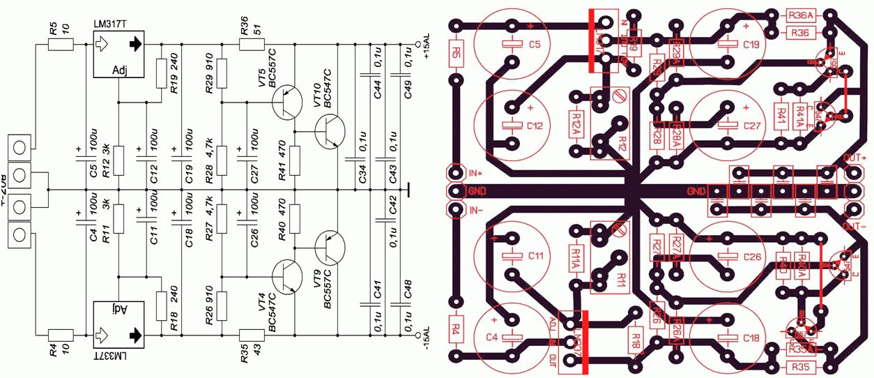
So far I only have copied layouts from present PCBs, but this is one of my first attempts to create a layout from a schematic. Here I just followed my intuition and tried to create a sort of star ground and get short traces. Differently from the schematic, I included some additional resistor pads for possible paralleling to obtain non-standard values. I also included the possibilty to use a trimmer at the adjust pins of the voltage regulators.
Please have a look and rate it. I'm not really sure how to translate the "parts sequence" of a schematic to a layout. Any hint is highly appreciated. Thanks in advance!
Please have a look and rate it. I'm not really sure how to translate the "parts sequence" of a schematic to a layout. Any hint is highly appreciated. Thanks in advance!
An externally hosted image should be here but it was not working when we last tested it.
An externally hosted image should be here but it was not working when we last tested it.
Last edited:
Hi
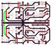
Tracks shown in red below should be replaced by tracks shown in green.
With the existing layout: Voltage ripple/spikes at the inputs cause current ripple/spikes through C4/5, which causes voltage ripple/spikes on C11/12 due to the shared copper tracks. This is bad as it injects garbage into the "adj" pins of the regulators.
Regards - Godfrey
Attachments
Not layout related, but you should add diodes to protect the regulator against discharge from the adjust and output caps - see data-sheet.
E.g.
http://tangentsoft.net/elec/tread/misc/sch-v1.1.pdf
(Tangent Regulator, Adjustable, plus Diode bridge)
E.g.
http://tangentsoft.net/elec/tread/misc/sch-v1.1.pdf
(Tangent Regulator, Adjustable, plus Diode bridge)
The star ground should start at the PS input connections. I prefer supplie lines to be wider traces ond common to be twice that width (where possible). I also prefer the most direct route of a connection, meaning abandoning "45s", especially in analog circuitry and most definetly in RF.
Onto the schematic drawing: Do not use X-type connections, only Ts. This is detailed in the ANSI and DIN standards. I know that even the most seasond designers do it, but after a few photo copies you may not see the connection or see one that is not there.
Enjoy pcb design and develop your creative side! E
What's a "45"?... meaning abandoning "45s", ...

I'm late - I've only just seen this...
What is the purpose of the VT5 VT11 section of this circuit ?
It does not appear to do anything useful - in fact, VT11 will burn up every time.
Anyway, R36 just makes the output resistance higher and also the load regulation will be degraded. I would delete the middle sections.
As others have already said:
You need suppression cap at the input pin of LM3x7 regulators.
With C18+19 at 100u, you need protection diodes between the LM3x7 regualtor's input and output pins.
With C11+12 at 100u, you need protection diodes between adjust and output pins.
These last 3 points are covered in the LM317/337 datasheets.
Rgds, Simon
This sounds like a Power Ground and a Signal Ground.Consider to create 2 GND's. 1 GND returning all of the DC rail coupling Caps + and -
The other one for the rest...
Do not return any dirty ground currents to the Signal Ground. eg. Zobel, Speaker, Relays, etc.
- Status
- This old topic is closed. If you want to reopen this topic, contact a moderator using the "Report Post" button.
- Home
- Design & Build
- Construction Tips
- From schematic to layout - Am I doing it right?