A ground plane is not intended to carry normal currents. So any connection to it should have its own path such that removal of the ground place does not disrupt operation.
It's basically a shield. Any current in it, other than outside generated noise, should be zero.
You can use short ground masses as ground points for individual stages. Connect all of them to the ground plane at one point.
It's basically a shield. Any current in it, other than outside generated noise, should be zero.
You can use short ground masses as ground points for individual stages. Connect all of them to the ground plane at one point.
If it is a digital design use a contigous (unbroken) ground plane. Star grounding is not for digital circuitry. This plane should not have slots in it either.
I'm must disagree with the comment about ground plane currents, ground planes are designed to carry the return current, and are critical in digital designs as the return current follows the path of least inductance, so will track under the signal route. In fact most digital designs these days are better with at least 4 layers, the inner two being a closely coupled power and ground planes.
An of interesting links. I have a few more.
http://www.elmac.co.uk/pdfs/Lord_of_the_board.pdf
A simple, low frequency, low power circuit may work regardless of layout. Power and ground planes usually cost money and effort. They are often used so that mass-produced items meet strict EMC regulations.
What frequency will your circuit operate at? How much power will it use? How complex is it?
It could be you are worrying about nothing...
w
What frequency will your circuit operate at? How much power will it use? How complex is it?
It could be you are worrying about nothing...
w
Granted lower frequency, slow rise time SIMPLE digital circuits will work on 2 layer with max copper pour for return currents. But you will get best results with a multilayer power and ground PCB. Most commercial designs are multilayer not only because of EMC issues but also for signal integrity. As for EMC it is an issue both for the internal circuitry as well as preventing it from getting to the outside world.
It is probably 10 years since I've done a two layer board (excluding flexis).
As well as overall operating frequency the signal rise time is important as it is fast rise times that cause more problems, as this determines the highest harmonic content of the square wave.
Also if you are building a DIY project I would go for the best, and with digital a contigous ground plane is best.
With the state of the PCB inductry in both USA and the UK it is surprising how cheap 4 layer boards can be, though you do require layout software that can handle 4 + layers.
Last edited:
Thank you for your advices.
I'm going to build a non-oversampling DAC, thus in the same chip there are both analog and digital signals. Max clock frequency is 12 MHz.
A 4 layer PCB is beyond my capabilities. I'm in doubt between these two solutions:
1) A two layer PCB, the first is used as a ground plane on the components side, and the second is used to route connections between components; negative power supply route is connected in one point to the ground plane (as suggested by bob91343).
2) The second solution is similar, but all ground connections are directly routed to the ground plane (ground returns spread all over the board).
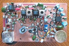
There might also be a third solution, mounting the components "Manhattan style", as many radio amateurs do to build their RF circuits (see the attached image). In this case there is only one layer, used as a ground plane and non-ground pins are soldered to small pads glued to the pcb.
Which solution is the best for my circuit? Are there other possibilities, given that the PCB has one or two layers?
Best regards.
Paul
I'm going to build a non-oversampling DAC, thus in the same chip there are both analog and digital signals. Max clock frequency is 12 MHz.
A 4 layer PCB is beyond my capabilities. I'm in doubt between these two solutions:
1) A two layer PCB, the first is used as a ground plane on the components side, and the second is used to route connections between components; negative power supply route is connected in one point to the ground plane (as suggested by bob91343).
2) The second solution is similar, but all ground connections are directly routed to the ground plane (ground returns spread all over the board).
There might also be a third solution, mounting the components "Manhattan style", as many radio amateurs do to build their RF circuits (see the attached image). In this case there is only one layer, used as a ground plane and non-ground pins are soldered to small pads glued to the pcb.
Which solution is the best for my circuit? Are there other possibilities, given that the PCB has one or two layers?
Best regards.
Paul
Attachments
Thank you for your advices.
I'm going to build a non-oversampling DAC, thus in the same chip there are both analog and digital signals. Max clock frequency is 12 MHz.
Since DACs support circuitry is 80% analog, the technique in the image s/b more than enough.
Usually you can find good suggestions on grounding, D/A interface techniques, and even PCB layout artwork in high speed DAC data sheets. I suggest you go there first.
Last edited:
I would keep the solder side as ground plane, treating it as though it has 2 sections divided along the line dividing the analog and digital pins on the DAC, all the analog components above the analog side and all the digital components above the digital side.
Now you can route power and signal connections on the component side, place your decoupling caps as close to the power pins as possible and drop their ground connections through to the ground plane.
In some ways it is better to have the ground plane on the component side, but this necessitates many vias to drop the signal and power connections through to the solder side if components are SMT.
Look at all the ground returns and make sure none cross from the digital to the analog sections. This may be affected by whether there are separate digital and analog power supplies, and it will have a major influence on where you make the connections from the PSU to the board.
w
What I have written is based on the presumption that the majority of components will be SMT.
Last edited:
Last edited:
Many thanks for the links and for the advices.
I'm going to build a DAC based on the old but well-reputed TDA1541A. I'd like to apply the suggestions from the (very long) thread http://www.diyaudio.com/forums/digi...building-ultimate-nos-dac-using-tda1541a.html.
I'm in doubt how to route the fourteen SMD capacitors used as a filter in the dynamic element matching circuit, which go from a pin of the IC to the analog ground. It's best to solder them directly to a ground plane, or provide a seprate route to the analog ground pin of the IC?
Best regards.
Paul
- Status
- This old topic is closed. If you want to reopen this topic, contact a moderator using the "Report Post" button.
- Home
- Design & Build
- Construction Tips
- Grounding scheme