Class D Amplifier Power Supply Design -> 12,5 A @ +/-80V = 1000W
hello guys
i'm going to build the biggest amplifier ever built by me
the main trouble is the power supply, a toroid is too much expensive and too much weight.
so i have decided for a switched mode power supply
i've found a design for a 700W power supply and i've modified it to deliver a maximum of 1000W, 80+80V.
here is the layout and the top and bottom layer, i'm searching for suggestions and improvments before producing the pcb.
of course is possible to order more pcb if you want one of them
Attachments
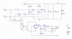
this is the second and the third part of the schematic
this is the layers and layout
An externally hosted image should be here but it was not working when we last tested it.
An externally hosted image should be here but it was not working when we last tested it.
this is the layers and layout
An externally hosted image should be here but it was not working when we last tested it.
An externally hosted image should be here but it was not working when we last tested it.
An externally hosted image should be here but it was not working when we last tested it.
some trouble with the links...
try to copy and paste this:
www.cronokart.com/images/images/sch2.JPG
www.cronokart.com/images/images/sch3.JPG
www.cronokart.com/images/images/bot.JPG
www.cronokart.com/images/images/top.JPG
www.cronokart.com/images/images/layout.JPG
try to copy and paste this:
www.cronokart.com/images/images/sch2.JPG
www.cronokart.com/images/images/sch3.JPG
www.cronokart.com/images/images/bot.JPG
www.cronokart.com/images/images/top.JPG
www.cronokart.com/images/images/layout.JPG
Hi Selfservice,
There are some errors in the attached schemas.
C72, C73, C76, C77 are misprinted, they need to be diodes. A graetz bridge, for that power a 600V/25A type is needed.
In the +/-12V supply a 7912 is needed in the lower side.
On the margin it looks an interesting project.
Regards,
There are some errors in the attached schemas.
C72, C73, C76, C77 are misprinted, they need to be diodes. A graetz bridge, for that power a 600V/25A type is needed.
In the +/-12V supply a 7912 is needed in the lower side.
On the margin it looks an interesting project.
Regards,
thank you for the quick reply!
for the graetz bridge there are faston connectors for the bridge to be applied on the heatsink via some cables, for simplyfing the layout.
for the -12V, cause is used only by the op-amps, i've decided to use only a resistor and a zener diode. the +12V is used also for the SG IC and so i've decided to stabilize it.
 Great looking project! If this turns out to be working well I'd definately be interested in building one!
the main transformer is an ETD59.
of course is possible to get +/-35V, but i don't know the efficency
there is the possibility lo regulate the output in fixed step of +/- 41 58 or 82 V, or via an external trimmer to have a variable regulation.
I hope to get the frist working prototype in the end of september, because the service of the pcbs are on holiday now.
now i'm going to build only 2 pcbs, because of $ carence, it will cost 95€ each but if you want we can order more pcb for lower cost, for example 15 pcbs will cost only 20€ each
of course is possible to get +/-35V, but i don't know the efficency
there is the possibility lo regulate the output in fixed step of +/- 41 58 or 82 V, or via an external trimmer to have a variable regulation.
I hope to get the frist working prototype in the end of september, because the service of the pcbs are on holiday now.
now i'm going to build only 2 pcbs, because of $ carence, it will cost 95€ each
but if you want we can order more pcb for lower cost, for example 15 pcbs will cost only 20€ eachwell i quess i have to test if my P3A will work on +/- 41V aswell but i think that wouldn't be a problem with my MJE15034 and MJE15035 output drivers..
Where are you planning to get the toroids. or maybe you are going to wind them yourself? if we can get 15 people. You can count me in!
Kind Regards Fix
Where are you planning to get the toroids. or maybe you are going to wind them yourself? if we can get 15 people. You can count me in!
Kind Regards Fix
95€ each
Is toroid expensive? Compared to what? I usually build a complete smps for that price!
_________________________________________
Some comments:
This is a very hazardous PCB design!!! Some regulations say a 230V powered device should have 8 mm creepage distance between high and low potential parts of circuit to avoid the risk of electric shock. Considerate this, when you redesign the layout, and check transformers if they can withstand at least 2 kV impulses or not!
75 ohm gate driver impedance is quite weak. This way switching transient lasts for about a whole microsec, which means significant power loss.
ETD59 is unneccessarily big for this power, but if you already have it, then you can choose higher number of turns, lower switching freq, consequentally smaller switching loss.
L1=350 uH? What kind of inductor can bear 12 A without saturation in that small size, and that high inductance? I don't know anything like this. You should decrease inductance significantly, and you shoud use common iron core in both chokes!
Where do you get 2200uF/600V from? Especially this tiny ones? 2*330uF/450V is perfectly enough.
A supply, which switches off at 1000 W instantaneous power, is enough only for a 2*200 W amplifier. It is advisable to allow much more instantanous current, than max. continuous current.
Voltage stabilizing is unneccesarily complicated.
Inrush current should be limited (by an NTC or simple resistor bypassed by a relay after ~1 sec).
for the pcbs is necessary to have a professional service because of the metallized holes and the heavy current on it, you cant'use a piece of wire soldered on the two layers, it will melt down.
the toroids and transformer nucleus and spole are avaiable via rs components, i'll post the complete bill of materials when the design is complete and fully ok.
but i'm still searching for suggestions on the pcb layout? anyone knows if and where i was wrong in the layout of the pcb?
the toroids and transformer nucleus and spole are avaiable via rs components, i'll post the complete bill of materials when the design is complete and fully ok.
but i'm still searching for suggestions on the pcb layout? anyone knows if and where i was wrong in the layout of the pcb?
hi pafi! we've posted together
well...
finally some improvments!
you are right, about the 8 mm distance, i haven't considerated it cause i've frist designed it only for my purposes, i'll never expect such interest about this project.
so i'm going to modify the layout considering this.
i've used etd59 because it's bigger allowing easier building of the windings, and because i can get it in easy way.
the 95€ is for 1 pcb, a prototype only, of course mass production cost less and less.
about the inductor: yes, it's quite impossible... i'll fix it
the 2200uf capacitor is obiviously impossible, in fact it's a 470uF 400V, there is a 2200uF cause to a too fast copy and paste
how to deliver more istantaneus current? suggestions?
what about the gate impedance? i don't understand...
Thanks Pafi !
...glad to read your safety advice.
Regarding the transformer the regulations are similar stringend as for the PCB and demand for the same creepages, clearances & min paths.
Or instead of distance/creepage/path also usually triple isolation layer are accepted, or in case of a single isolation a min thickness around 0.5mm (not sure about the exact value and which materials are not allowed...). From what I know the high pot requirements are at least 4kV.
Please don't fully rely on my words, I did not go through all relevant details of your particular design and the related safety standards. Requirements might be even more tough. You never know what some people put into hidden corners of these standards...
Regarding the size of the trafo.
Be happy that you have that large size. It might give you a chance to design it with proper isolation.
Take care especially for paths like:
winding ==> winding, margin tapes are helpful
winding ==> core ==> winding
pin/wiring ==> core ==> pin/wiring
....
Such trafos are ugly 3 dimensional beasts, which tend to trick our brain.
ChocoHolic!
I have no reliable info on hi pot requirements, I heard about different ratings, but 2 kV is the least. One should try to achieve as much as possible, and then test it. This is not production, only DIY.
Grounding (protective earth) of output 0 improves safety. If 4 kV withstand can't be reached, then this can be a solution.
There is a wire with isolation qualified to >4 kV strength, and it has only ~0,2 mm thick isolation. I have it, but I don't know its name. It's yellow. For unisolated parts a layer of clean silicone rubber can do the job.
Selfservice!
A gate have 60-70 nC charge. If you want to turn off in eg. 100 ns, you have to sink I=dQ/dt=600-700 mA. This is obviously impossible through 75 ohms. But saidly gate resistor is not the only limiting factor, SG3525 is too weak too, and transformer is problematic too (it has leakage inductance). You have to make experiments on this.
You can insert a RC network into the current sense circuit.
Yes, but it worths the efforts.
I have no reliable info on hi pot requirements, I heard about different ratings, but 2 kV is the least. One should try to achieve as much as possible, and then test it. This is not production, only DIY.
Grounding (protective earth) of output 0 improves safety. If 4 kV withstand can't be reached, then this can be a solution.
There is a wire with isolation qualified to >4 kV strength, and it has only ~0,2 mm thick isolation. I have it, but I don't know its name. It's yellow.
For unisolated parts a layer of clean silicone rubber can do the job. Selfservice!
what about the gate impedance? i don't understand...
A gate have 60-70 nC charge. If you want to turn off in eg. 100 ns, you have to sink I=dQ/dt=600-700 mA. This is obviously impossible through 75 ohms. But saidly gate resistor is not the only limiting factor, SG3525 is too weak too, and transformer is problematic too (it has leakage inductance). You have to make experiments on this.
how to deliver more istantaneus current? suggestions?
You can insert a RC network into the current sense circuit.
optocoupler? that's require a massive redesign...
Yes, but it worths the efforts.
- Status
- This old topic is closed. If you want to reopen this topic, contact a moderator using the "Report Post" button.
- Home
- Amplifiers
- Class D
- Class D Amplifier Power Supply Design -> 12,5 A @ +/-80V = 1000W