Hi,
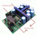
I was looking at the layout for the UcD700 from Hypex and it would appear the output inductor and modulator are quite the distance away from the MOSFETS.... I'm no skilled PCB designer and I know the people at Hypex know what they are doing so my question is how can they get away with it? It seems counterintuitive to have the inductor almost a full PCB length away from the MOSFETS at 700W RMS.
Thanks,
-=Randy Knutson
Mankato MN
Attachments
It looks like the output inductor is only about 2" away from the fets, which isn't too far considering all of the components that are packed on both sides of the pcb. You're right that the ideal layout would keep the trace carrying the switching current between the fets and inductor as short as possible, but PCB design is all about the art of compromise.
Do you mean to imply they are setting up some sort of transmission line between the MOSFET and inductor using a multi-layer PCB? Or that using more layers increases current carrying capability of a thin trace without significantly increasing trace inductance?
Thanks,
-=Randy
Thanks,
-=Randy
When implemented properly, boards with more copper layers can offer better EM shielding. Of course the inner copper layers are thinner and inner traces have to be a bit wider than normal outer layer traces if they need to carry a lot of current.
I think Chris implied that they may be using a snubber to deal with the increased voltage and current spikes caused by the inductance of a longer switching trace. I don't want to put words in his mouth though")
I think Chris implied that they may be using a snubber to deal with the increased voltage and current spikes caused by the inductance of a longer switching trace. I don't want to put words in his mouth though
More board layers mean you can use an uncut gound plane for the entire current loop of the output stage. Using uncut ground planes the size of the output trace loop means that the inductance of this loop is lowered a great deal, something very difficult to achieve in only 2 layers :/
- Status
- This old topic is closed. If you want to reopen this topic, contact a moderator using the "Report Post" button.
- Home
- Amplifiers
- Class D
- UcD700 PCB Layout Question