Eva said:Open loop digital systems are a big no-no, a stupid dead-end
Power Supply Rejection Ratio is 0dB in these systems!!
On the other hand, closed loop digital systems are equivalent to any analog-controlled class D amplifier, but requiring fast, precise and expensive ADCs instead of standard DACs, so they are another dead end.
Hi Eva!
How could you define the 0 dB PSRR with a full-bridged amp.?
PowerDAC3 development
Hi all
I have several photos of prototypes and pcb version of my new PowerDAC3 digital amplifier power module that when zipped result in a file of around 1.8MB.
I'd like to post these on the forum but the 100K attachment limit poses a problem. I've tried reducing the image size or jpg quality of these images so that each is less than 100K, but I feel the loss of detail is too great. As you know, with things like this the devil is in the detail.
Does anyone have any ideas on how to work around this in some way that does not compromise image quality?
PowerDAC3 development
Here follow some photos of the PowerDAC3 prototype which I designed and built around 18 months ago, and first pcb version which I am presently testing.
Thanks to Al for compressing the pics for me without losing detail.
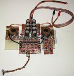
Proto1.jpg
Proto2.jpg
These show the single channel prototype OPS of the PowerDAC3 about halfway through development.
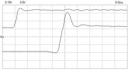
FDS3672phase2.jpg
This scope photo shows the 3.3V PWM logic drive signal and the OPS switching waveform on the OPS phase node at Vdc = 15V. Signal integrity is preserved over the full Vdc range of 1-60V.
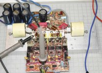
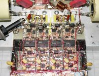
Proto3a.jpg
Proto3c.jpg
Proto3d.jpg
These show the single channel OPS of the PowerDAC3 in the final prototype configuration completed around 18 months ago and which was taken to pcb. The OPS is an open-loop full bridge using SMD power devices and was tested to 350W into 4 ohms, 175W into 8 ohms. THD+N was around the 0.02% mark at all powers and efficiency was over 98%. The four discrete gate drivers are clearly visible in centre field, and the circuitry on the right hand side is output overload monitoring.
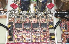
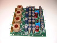
Pmod debugging.jpg
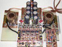
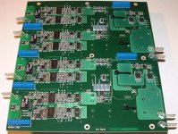
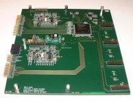
This shows the first pcb version of the PowerDAC3 Stereo Power Module which incorporates two of the OPS circuits from the protos, each of which has its own SMPS voltage regulator. The OPS feature an adaptive 'calibration algorithm' which is used to electronically optimise output stage switch timing and so eliminate the effects of ageing and parameter spread in MOSFet switching. The average current mode SMPS switch at the PWM switching frequency of 352,8kHz and are rated at 60V 10A continuous. They have an analog control loop with digital adaptive loop control, digital reference generation and supervision. PWM values are sent to the modulator in the form of signed 8-bit numbers from an external host, via a synchronous LVDS data interface. The Power Module incorporates a low-jitter reference clock synthesiser and a stereo PWM modulator. Regulator control, system monitoring, self-tests, and OPS calibration and is via a synchromous LVDS control interface.
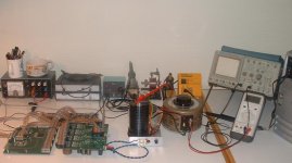
The Power Module consists of two pcbs, namely an upper power board and a lower control board. These are normally mounted in a stack with standoff pillars between the two boards and interconnection via headers and header sockets. In the photo taken last December the two boards are separated during debugging and testing for access to components, and the interconnections are made with ribbon cable harnesses. Testing is still in progress. (Jan 2008)
All logic and control of the OPS and SMPS regulators, conversion of analog parameters for calibration, PWM generation and control is implemented in a single Actel Fusion FPGA which can clearly seen on the control board. Only the SMPS control loop core is implemented in analog.
This pic is proto1.jpg
Here follow some photos of the PowerDAC3 prototype which I designed and built around 18 months ago, and first pcb version which I am presently testing.
Thanks to Al for compressing the pics for me without losing detail.
Proto1.jpg
Proto2.jpg
These show the single channel prototype OPS of the PowerDAC3 about halfway through development.
FDS3672phase2.jpg
This scope photo shows the 3.3V PWM logic drive signal and the OPS switching waveform on the OPS phase node at Vdc = 15V. Signal integrity is preserved over the full Vdc range of 1-60V.
Proto3a.jpg
Proto3c.jpg
Proto3d.jpg
These show the single channel OPS of the PowerDAC3 in the final prototype configuration completed around 18 months ago and which was taken to pcb. The OPS is an open-loop full bridge using SMD power devices and was tested to 350W into 4 ohms, 175W into 8 ohms. THD+N was around the 0.02% mark at all powers and efficiency was over 98%. The four discrete gate drivers are clearly visible in centre field, and the circuitry on the right hand side is output overload monitoring.
Pmod debugging.jpg
This shows the first pcb version of the PowerDAC3 Stereo Power Module which incorporates two of the OPS circuits from the protos, each of which has its own SMPS voltage regulator. The OPS feature an adaptive 'calibration algorithm' which is used to electronically optimise output stage switch timing and so eliminate the effects of ageing and parameter spread in MOSFet switching. The average current mode SMPS switch at the PWM switching frequency of 352,8kHz and are rated at 60V 10A continuous. They have an analog control loop with digital adaptive loop control, digital reference generation and supervision. PWM values are sent to the modulator in the form of signed 8-bit numbers from an external host, via a synchronous LVDS data interface. The Power Module incorporates a low-jitter reference clock synthesiser and a stereo PWM modulator. Regulator control, system monitoring, self-tests, and OPS calibration and is via a synchromous LVDS control interface.
The Power Module consists of two pcbs, namely an upper power board and a lower control board. These are normally mounted in a stack with standoff pillars between the two boards and interconnection via headers and header sockets. In the photo taken last December the two boards are separated during debugging and testing for access to components, and the interconnections are made with ribbon cable harnesses. Testing is still in progress. (Jan 2008)
All logic and control of the OPS and SMPS regulators, conversion of analog parameters for calibration, PWM generation and control is implemented in a single Actel Fusion FPGA which can clearly seen on the control board. Only the SMPS control loop core is implemented in analog.
This pic is proto1.jpg
Attachments
Actually, the lower switching frequency has lower distortion and better efficiency but can not handle the higher frequency range of full band audio. That is why you aren't seeing so much really high carrier frequencies. You are starting to see some, but that is due to the consumer electronics companies needing to lower thier costs by using smaller inductors. You will also see more single ended class D amps for the same reason (less inductors, lower cost) but power supply design is much more complicated due to supply pumping and you lose the advantage of the carrier being cancelled out across the load because it's common mode.
The reason for the higher efficiency and lower distortion with lower switching frequencies is this:
A major loss in class D amps is the transistion from low to high or high to low, This is also where a lot of the output stage THD come from. This is where the MOSFETs must travel through thier linear region and have a small amount of cross conduction. With a lower switching frequency, this happens less amount of times per second. The more times per second you are in the linear region the more heat you will be dissipating. Also since the transition is never instant. The rise and fall time of the transition is introduced as THD. Again the more time per second this happens the higher the THD. As far as the rise and fall times, that is why the more cross conduction you have, the lower the THD you will have (Up to a limit). But of course more cross conduction = less efficiency and higher noise levels. These are the trade offs you can make for yourself if you design your own output stage. With the TI chips, you can take the PWM modulator output and put it into your own power stage, and conversely take a TI power stage and create your own analog modulator if you want an analog input class D amp (which I still believe is better than completely digital) but of course you will need to build your own PSRR (feed forward correction) circuit and feedback if you want to use it with a linear supply.
Dave
Performance of switching amps
Yes, all this is true.
What's also true is that at the present time, open loop digitally modulated and even most closed loop Class D amps don't approach the state of the art in terms of THD or S/N.
(John Westlake's closed loop digital amp may be an exception to this, though)
Infuriatingly, the top hand seems to stilll held by analog power stages. One of the interesting developments I've come across here is the National Semiconductor LME49810 analog power amp driver chip which when used with complementary bipolar output transistors leads to a simple power amp of 500W with THD around 0.0006%.
So, one can knock together something like this in a few weeks. Or you can spend 12 years designing a series of the most complex and critical to get right amplifiers known to man and teach yourself a myriad of useful design skills along the way?
(John Westlake's closed loop digital amp may be an exception to this, though)
Is John's amplifier in production by now?
Re: Performance of switching amps
It's the journey that counts, not the destination")
Jan Didden
John Hope said:Yes, all this is true.
What's also true is that at the present time, open loop digitally modulated and even most closed loop Class D amps don't approach the state of the art in terms of THD or S/N.
(John Westlake's closed loop digital amp may be an exception to this, though)
Infuriatingly, the top hand seems to stilll held by analog power stages. One of the interesting developments I've come across here is the National Semiconductor LME49810 analog power amp driver chip which when used with complementary bipolar output transistors leads to a simple power amp of 500W with THD around 0.0006%.
So, one can knock together something like this in a few weeks. Or you can spend 12 years designing a series of the most complex and critical to get right amplifiers known to man and teach yourself a myriad of useful design skills along the way?
It's the journey that counts, not the destination
Jan Didden
PowerDAC3 sings!
I have completed the testing on my PowerDAC3 digital amplifier power module. It checks out really good, with THD around the 0.02 - 0.03% mark 20-20kHz at all powers into 4-8 ohms. I am very happy with the power circuitry now and will not make any further changes to the power pcb.
The control pcb also functions as planned.
For testing and audition I fed it with serial streams of 8-bit 'PWM numbers' derived from the signal processing chain in my PowerDAC 1 digital amplifier. It sounds better than any of the previous PowerDACs I have made and has truly effortless punch.
I'll post some pics sometime soon.
The Actel Fusion AFS600PQ208 FPGA in the control board gave me a lot of trouble. It's a very new device and not properly in production yet. Actel have taken nearly a year to get this device going and they still aren't there. Some of the functionality was lacking in the REV D silicon. Then the s.o.b. failed to properly program its flash after about 30-50 reprogs, so the claimed 500 cycles flash write endurance Actel specifies is still wishful thinking. The other REV D specimen I'd been given had yet other functionality missing, but fortunately not enough to impede my progress towards music!. I've been promised by Actel a fully working REV E device by mid April, but by now I am 'gatvol' of this FPGA and I've decided to redesign the control board of the amp to use a more reassuringly familiar Altera Cyclone II device.
What influenced my decision was the fact that the EMC environment proved benign and the present FPGA logic in the Actel functioned flawlessly on the lower board only a few cm from where up to 10A 60V is being switched in 5ns on the power board above (with no ringing!)
So I thought in the light of this why not go the whole hog and make more than a Power Module that still requires external signal processing - why not offload ALL the signal processing and supervisory functions (that I was going to do in a separate processing module) onto a new drop-in processing board that will take I2S or AES in from source and stack with the preset power board. This would make a really attractive OEM digital amplifier module. So this is what I'm doing.
More on this story later, as they say on the news. . .
Great work John on this amplifier - it seems like a tremendous amount of work judging by the PCB photos - are these wire-wrap connections between parts? Will the final design be a commercially available product or incorporated into one?
As to PS design, I have done some tests with battery power (12V 7aH SLA) into the output stage of a Panasonic SA-XR57 Equibit amp & I didn't find an improvement in the sound, in fact it lost some punch to the sound compared to the mains PS. http://www.diyaudio.com/forums/showthread.php?postid=1461455#post1461455
The mains is fed through a step-down isolation transformer (240V to 110V) which I believe, at the moment, is what gives the amp a better sound than the battery! I will be testing further with paralleled batteries to increase the current.
I attach the PS schematic from the SA-XR57 amp for your perusal (the variable control of the PS voltage is circled). Panasonic have changed the this PS circuit from the one that was used in the XR45 & mentioned by Kims further back in the thread. The XR45 PS (considered to be the best sounding) used a DC-DC converter as the control element.
Koon seems to favour a discrete PS vol control over a SMPS one http://koonlab.com/TAS4i.html
Any comments?
Attachments
- Status
- This old topic is closed. If you want to reopen this topic, contact a moderator using the "Report Post" button.
- Home
- Amplifiers
- Class D
- Anyone interested in a digital amplifier project?