Bruno Putzeys said:
...Hmmmm... I've often dreamt about making an adaptive control circuit that made for negative dead time so it always crosses over precisely at Id=Iout. Hugely interesting, both in terms of distortion and efficiency, but "fairly" impractical.
<snip>
This is quite obvious. As long as the FET is transitioning (Vds is moving down), the miller effect will insure that Vgs cannot move beyond the point corresponding with drain current.
It's quite simple, isn't it? If Vds>>0, Id is determined only by Vgs. If Vgs were higher, either Vds should be 0 or there should be shoot-through preventing Vds from coming down.
As I explained in private earlier, I try to point people in the right direction, without giving recipes. Recipes do not constitute "understanding". Understanding comes only through study, experimentation, and at times a friendly hint from others.
There are too many people around who try to cream recipes from forums such as these in order to get into the market with their "own" designs quickly, without feeling the need to understand what they're doing. I don't feel any need to give these people a cheap ride by writing a "how-to" guide.
However, there are a few folks out here who themselves work and study hard to gain a proper in-depth understanding. There, it makes little sense to withold information. You yourself, for instance, will find out these things in due time anyway. So then I think it's worth to give nudges in the right direction, knowing full well that these hints won't be understood by people simply looking for a quick design help.
Yeah you know it's hard for someone in my situation to fully understand that fine line upon which you dance, even though I think I can.
Maybe in light of that next time just dont' say "I'm now withholding useful information..." just to make it easier on us?
All the same, yeah those leeches are around, I'd like to think anyone like that would fall on their face hard and fast. Like you say, there's only one way it can be done, it takes work.
I also appreciate that your hints usually are in the right direction as well. Usually.... well black gates are expensive anyway, I wont' even count that
")
I've dreamt of the same type of dead time control, maybe. Spent a few good hours researching that as well.
When you say negative dead time I'm thinking of predictive.... same thing?
The conclusion was very much like yours, but will remain in the back of my mind for later consideration. All the same I can't help but wonder what made _you_ classify it as being fairly impractical... was it the required reaction time for it to actually be functional? Still a good idea, if we are talking about the same thing.
It's almost looking like a waste of time to worry about dead time at all.
I trust we can ignore that Vth differs from device to device, thanks to a good manufacturing process.
So then we'd want to limite the rail current as we're playing with dead time .... so they'll be running cooler and have a higher threshold than they would in normal use... would you heat the devices externally to lower Vth closer to what it would be in normal operation?
It actually looks at this point like all one can do is tune it to be optimal at idle and hope for the best at higher output, where you're actually listening to it most of the time.
Lately I've just been concentrating my efforts on having the gate signals intersect at Vth, and at least in simulation this gives best results, and is the same as having zero dead time. With that relation in good form we dont' really need "dead time".... do we?
Seems like it's too much of a carry over from the digital only days.
Now if any of this is a song you can't dance to on here I'd appreciate if you late me know privately or whatever.
BTW Bruno, thought you'd get a kick out of knowing that since I moved at least 10 people have heard my little home brew UCD simple as can be version, only one i've built, and 10 jaws have dropped.
Best Regards,
Chris
Precisely. In its original meaning, "Dead time" is used to denote an intentional delay between turning off one FET and turning on the other, presuming gate switching time to be negligible compared to the intentional delay. This is typically true for designs that have optimal idle current. The delays we are looking at for normal use (higher idle losses, lower THD) are so much shorter that the FET switching time becomes dominant. Because of that, it makes little sense to try and distill a single figure. Even if you cross over at Vth, you will find distortion artefacts typical of dead time.classd4sure said:Lately I've just been concentrating my efforts on having the gate signals intersect at Vth, and at least in simulation this gives best results, and is the same as having zero dead time. With that relation in good form we dont' really need "dead time".... do we?
Crossing over at Vth is a practical proposition using P/N mosfets capacitively coupled to a shared gate driver, or less practical, using a drive transformer coupling all gates.
Bruno Putzeys said:
Most power FETs have metal gates. If they were polysilicon they'd be too slow for use in class D. The lead inductances form the limiting factor towards direct readout of the gate waveform. At realistic gate switching speeds (50-100ns), the fidelity of the waveform at the gate pin is still more than sufficient. Faster switching speeds make no sense if the dead time is long enough to be seen as a diode drop on the scope screen.
WHAT? METAL GATES??? what about vacuum tubes?
I'd say 99.999% of power FETs have poly gate. I am not aware of ANY power FETs still using metal gates. Most use low resistivity poly (aka silicide). All power FETs these days use self-aligned poly gate.
Faster switching speed reduces the time the FET is in saturation, where the switched node is half way between the rails, and the FET is dissipating a lot of power. The faster the better, but worse for EMI. You don't lose power for switching faster. Remember RC charging requires same energy regardless of its time constant.
All power ICs generates a good definitive blip, at least 20ns, as long as 60ns or more. Some even prefer longer than shorter, just so they sleep better. Enough said. No more free consulting.
tawen_mei said:I'd say 99.999% of power FETs have poly gate. I am not aware of ANY power FETs still using metal gates. Most use low resistivity poly (aka silicide). All power FETs these days use self-aligned poly gate.
I agree with you, I've worked with a few larger MOSFET’s manufactures to help them understand the requirements of MOSFET’s for Class D, and NON use Metal Gate layers... although at times I wished they did....
A metal layer is used to distribute the Gate signal around the periphery of the MOSEFT die, with “fingers” distributing the signal into the die centre – however to maximize the RdsON vers Die area, the area spared for these “fingers” is limited.
Using a current probe on the MOSFET's Gate reveals some VERY interesting results.... I use ultra small current probes design for Laser Diodes....
John
Hi John,
do you mean something like EMI sniffer probes from Bruce Carsten?
Best regards,
Jaka Racman
do you mean something like EMI sniffer probes from Bruce Carsten?
Best regards,
Jaka Racman
Hi Jaka,
No I don't use the interesting little "sniffer" probes you posted - but these (see attached PDF) - I find they have much better performance then there Spec sheet. I've had these for years - I'm sorry, but I have no idea who Made / Makes them as its not indicated on the Data sheet...
I once measured some SMALL 30V MOSFETs that required almost 300nS to be fully enhanced (until the Gate stopped requiring current). Turns out the manufacturer had a major issue with there polysilicon implantation process - could not implant within the “deep” trench... Due the the common measurement Spec. of 10% to 90% Rise / Fall time - the manufacturer had completely missed the fact that the last 5% or so of Turn-on was taking a lifetime... and when your normally looking at the first 20nS or so of the switching event - its easy to miss the VERY gradual slope over 300nS!!
Needless to say these devices had very poor THD performance (odd-order components).
Cheers,
John
Attachments
tawen_mei said:WHAT? METAL GATES??? what about vacuum tubes?
I'd say 99.999% of power FETs have poly gate. I am not aware of ANY power FETs still using metal gates. Most use low resistivity poly (aka silicide). All power FETs these days use self-aligned poly gate.
Ok, ok, my gig is making amplifiers, not FETs. But, since your point was to say that gate resistance was a significant factor, I wouldn't mind seeing a number stuck to that.
Ivan how come you can't read the gate waveform ?
Preferably, do what you have to do so you can read the gate waveform...
What I did was simply used temperature and sound cleanliness, that amp now has over 100 hours on it, easily.
Using older mosfets can be a huge help in preliminary testing, they slow things down imposing a soft dead time and also limits EMI, which you notice if it's a problem or not real fast. IRF640 has proven to be a true workhorse for these stages of testing, and take an unbelievable amount of abuse, more than enough to get you into the ballpark for testing with more optimal mosfets.
At which point I'd strongly suggest limiting gate driver voltage so that Vgs only see's enough to fully enhance it and no more, this is also to help limite EMI and the possibility of ringing.
Regards,
Chris
Chris,
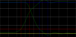
i talk about chip solutions, where gates isn't accessible. I've tried resistive load totem pole, but can't see the dead time exactly. This is switching wave form (10ns/div) for the TDA8939, which claimed zero dead time, because rise/fall edges 20ns>10ns as dead time. So i want to check others accessible chips, just by looking to the totem pole switching. How?
i talk about chip solutions, where gates isn't accessible. I've tried resistive load totem pole, but can't see the dead time exactly. This is switching wave form (10ns/div) for the TDA8939, which claimed zero dead time, because rise/fall edges 20ns>10ns as dead time. So i want to check others accessible chips, just by looking to the totem pole switching. How?
Attachments
Hi Ivan,
Consider the following. Dead time manifests itself in various ways in the actual behaviour of the power stage. You might try to list a few of the most important ones and see if any of them are measurable, either on a fully operational amp or on a test circuit.
For example, on amplifiers with a clear "dead time hump" in the THD vs power response, extrapolation of the right hand slope of the hump to the clipping point allows you to calculate dead time with good accuracy (if you know the loop gain of course - open loop amps are easier in this respect). Dead time on the TDA8939 is too short for this though, but there are other even more direct metrics.
Nice input, Bruno. But for such wise DT measurement, i need already well designed PCB for each chip, it so hard for me.. more direct -more attractive. This is switching screenshot for loaded(~15ns)/unloaded(~20ns) same chip (20uHn/1uF/8Ohm), it seems that DT is really zero Well, I'll try to compare the rise vs fall edges for DC at the output..(pumping- scary movie).
Well, I'll try to compare the rise vs fall edges for DC at the output..(pumping- scary movie).Attachments
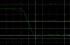
Considering that the switching behaviour of the chip will depend to some extent on the PCB layout, trying to determine "dead time" on a chip without a good PCB does not produce reliable readings.IVX said:Nice input, Bruno. But for such wise DT measurement, i need already well designed PCB for each chip, it so hard for me.. more direct -more attractive. This is switching screenshot for loaded(~15ns)/unloaded(~20ns) same chip (20uHn/1uF/8Ohm), it seems that DT is really zero
Your scope plot shows differences in rise time, but not where the edge is with respect to the actual dead time... Triggering on the switching waveform itself is not informative.
Such kind of PCB.. yeah, it's not given to me easily.
Actually, some assymmetry is well seen when "playing" DC. Just by fast looking (visual integration) the assymmetry maybe equivalent 5ns or less. I suspect, that also can try to read the driver supply current (boot strap pin), at least, in the simulation this current do things visible, however it is driver design depended.
Actually, some assymmetry is well seen when "playing" DC. Just by fast looking (visual integration) the assymmetry maybe equivalent 5ns or less. I suspect, that also can try to read the driver supply current (boot strap pin), at least, in the simulation this current do things visible, however it is driver design depended.
Ivan,
I was thinking of checking the ripple on the stab pins as well, but didn't think it would really tell the story.
Alternatively if you really wanna find out peel the top off the IC and take a thermograph to find the mosfets then you can probe it at the gate But how bad do you really wanna know? Can't ajust it anyway.
I was thinking of checking the ripple on the stab pins as well, but didn't think it would really tell the story.
Alternatively if you really wanna find out peel the top off the IC and take a thermograph to find the mosfets then you can probe it at the gate
But how bad do you really wanna know? Can't ajust it anyway.classd4sure said:Alternatively if you really wanna find out peel the top off the IC and take a thermograph to find the mosfets then you can probe it at the gate
You can see where the mosfets are even with your bare eyes. No need to pull out a thermograph. These don't have a very high resolution.
I remember once, with an early version of the TDA8920, we were trying to get Ph Semicon to make smaller gate drive buffers (the EMI of the first chips was horrendous). So they made a set of test chips with various gate fet sizes to see which was best. Well, one chip was marked as having small drive fets but it radiated abnormally. Unfortunately the IC blew so that was the end of the test. I then decided to strip the IC. That is, I clamped it in a vise and knocked the top half off the package using a hammer and a chisel. The chip was reduced to bits, but the epoxy still carried the chip's imprint on it. The imprint was good enough to show, under moderate magnification, that the gate drivers were indeed large.
So, if you do manage to get at the die, knowing where to probe is not a big problem. Knowing how is another matter, because the IC is glass passivated. You'd need to etch a hole through this layer before you can measure anything.
Chris, thanks,
your suggestion about a thermograph is really extraordinary.
BTW, i still can't find any offers for PWM controller before TDA8939 (here available ~5euro) at the www.philips.semicondcutors.com.
>1 year after press release..
your suggestion about a thermograph is really extraordinary.
BTW, i still can't find any offers for PWM controller before TDA8939 (here available ~5euro) at the www.philips.semicondcutors.com.
>1 year after press release..
MOSfet switching explained
International Rectifier's Application Note 947 is a comprehensive article on MOSfet switching and worth wading through if you really want to understand the true grit of this matter. It's a bit of a mathematical horror, and is best studied over a period of a few days. With the aid of a glass of good red wine. In silence.
http://www.irf.com/technical-info/appnotes/an-947.pdf
- Status
- This old topic is closed. If you want to reopen this topic, contact a moderator using the "Report Post" button.
- Home
- Amplifiers
- Class D
- Measuring deadtime