Sorry, analogspiceman, it was not my intention if I even thought it were possible to upstage you. I am considering the simplest but most effective circuit for me in my class D amplifier project, given my design constraints, and I am considering possibilities still. I can most easily both limit input amplitude and frequency, but I am considering throwing in a weaker than standard RC damper for good measure. The formula gives an R value of 6.8 and a C of 2.2uF. That may be one reason why I reduced the capacitor very much from optimal, as the power dissipation in the resistor is already about 10 watts, unless I misread the formula. Thanks, best regards.
This idea sounds a little more thorough than the idea I have simulated which uses two emitter followed voltage dividers from the amplifier power supply to power the input opamp. The values of the outer resistors can be equal to the feedback resistor and the inner resistors slightly more than the gain setting resistor to account for Vbe and opamp output that is less than rail to rail.
analogspiceman wrote
Actively peak track and low pass filter the lowest points of power supply ripple. Further reduce this by a signal proportional to mosfet current (compensates for IR drop). Scaled down just a bit, this then becomes a moving reference for an input limiter that always allows maximum possible output power (with no hum during "clipping"), and without ever having the output stage actually saturate and suffer the ill effects of opening the feedback loop.
This idea sounds a little more thorough than the idea I have simulated which uses two emitter followed voltage dividers from the amplifier power supply to power the input opamp. The values of the outer resistors can be equal to the feedback resistor and the inner resistors slightly more than the gain setting resistor to account for Vbe and opamp output that is less than rail to rail.
I wonder if the clipper I tried would track power supply ripple better if filter capacitors were tied from the bases to the power amp supply rails, plus two more from there to ground. It would make a capacitive voltage divider across the resistive one. It might not help, though.
Hello analogspiceman.


The crucial point is diode recovery of the outgoing fet. As long as this is still happening, dV/dt is very low so controlling it will have no effect on the speed at which the incoming FET tries to pull the outgoing diode open.
Needless to say I've got another trick that effectively combats this. I use it on all designs 200W and above.
")
Cheers,
Bruno
A-men. Anything that doesn't produce a neat triangle wave at the comparator produces non-linear modulation. That rules out anything except the simplest first-order schemes.analogspiceman said:Hi Bruno,
(at least at 50 percent duty cycle and as long as the signal appearing at the UcD input is more or less a sine wave).
Indeed, although the peaking produced by the reduced phase margin coincides with the switching frequency, which is why you only see it in the linearised model. Doesn't seem to mean much in practice as the amp is already oscillating at that frequency.analogspiceman said:Delays in the power stage (or right half plane zeros) eat your phase margin without giving back more loop gain, so a responsive power stage with a 3rd order type circuit would be best.
Not during normal operation. The inputs are only seeing the small oscillation wave form, which is quite a bit less than 5V (a few 10mV or so). However, I've indeed had to add diodes in some cases where even in the shutdown state (tail source off) very large signals like turn-on spikes of the preceding audio circuitry were capable of driving current into the input transistors (through be zenering into the emitter of the other transistor), producing cracking noises in the speaker.analogspiceman said:
Depending on what's driving it and how the inputs are configured, the UcD might need something (couple of diodes) to keep the input BE junction from Zenering.
Pure dv/dt doesn't bother me. Proper layout and correct choice of coil allow very large dv/dt's without causing detectable EMI. It's dI/dt that causes problems.analogspiceman said:
Also, with mosfets that need it (or to limit EMI), you might find my simple drain-to-gate RC dv/dt limiter useful, since the UcD is already set up perfectly with asymmetrical drive (its got the pull-down PNP that the RC needs so it only affects turn on dv/dt).
The crucial point is diode recovery of the outgoing fet. As long as this is still happening, dV/dt is very low so controlling it will have no effect on the speed at which the incoming FET tries to pull the outgoing diode open.
Needless to say I've got another trick that effectively combats this. I use it on all designs 200W and above.
Notedanalogspiceman said:(please tell Jan-Peter that if you get too busy with other projects, I'm ready to step in).

Cheers,
Bruno
Well if you are very patient and have enough power devices to spend on failed amplifier you could just possibly get a UcD based ampliverter working.Jaka Racman said:Hi,
Recently I discovered US patent 4479175 which has now expired. It renewed my interest in ampliverters. Since they work constant frequency, UcD control is out of the question.
Let's say I would not recommend it but just for the heck of it, here's how it could be done (mono amplifiers only):
1. Make a normal UcD loop.
2. Feed the comparator output to a state machine that alternatively switches the primary and secondary sides.
But here's the annoying bit:
3. Add a protection that will override the comparator output if it hasn't switched for the last few microseconds. Otherwise the primary side will blow instantly when the amp is clipped.
I'm not a fan of ampliverters though. The idea is very elegant, but the bilateral switches on the secondary side make things a bit more complicated in reality than in concept.
Cheers,
Bruno
Hi all,
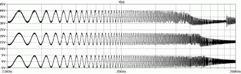
The attached gif file is the large signal frequency response analysis output from an LTspice simulation of an UcD180 style class d amplifier.
This simulation uses the recently derived mathematically correct swept sine time domain LTspice B-source in conjunction with a very fast running LTspice A-device to analyze the large signal behavior of a self oscillating class d amplifier under a variety of dc bias levels (approximates high frequencies riding on a large bass signal). The sine source is swept logarithmically from 2.5kHz to 250kHz (25kHz is center screen).
Many weird large signal effects (such as frequency shift, aliasing, pulling and lock) are clearly visible. Note that none of these would be evident in a small signal ac analysis.
When properly set up, the A-device simulates a realistic delay while efficiently allowing maximum step size between switching edges and simultaneously capturing edge timing with great fidelity. This makes successive design iterations possible with almost no waiting.
Time permitting, I will follow up with a post of a similar example based on my leapfrog design method to compare performance under difficult large signal conditions.
I also have a swept sine example of a highly accurate speaker model driven by an amplifier with realistic current and voltage limits modeled. This provocative simulation clearly shows why current limiting (even with perfectly flat and clean clipping) sounds much worse than voltage limiting.
Regards -- analogspiceman
Attachments
Here is the LTspice schematic file (mind the unintended word wrap).
Version 4
SHEET 1 1324 680
WIRE 64 16 64 -64
WIRE 64 128 64 96
WIRE 64 256 64 224
WIRE 64 368 64 336
WIRE 96 -64 64 -64
WIRE 96 224 64 224
WIRE 112 -64 96 -64
WIRE 112 224 96 224
WIRE 224 -64 192 -64
WIRE 224 -64 224 -160
WIRE 240 -160 224 -160
WIRE 256 -64 224 -64
WIRE 256 16 256 -64
WIRE 256 32 256 16
WIRE 256 128 256 96
WIRE 288 -64 256 -64
WIRE 336 -160 320 -160
WIRE 368 16 256 16
WIRE 416 -160 400 -160
WIRE 416 -64 368 -64
WIRE 416 -64 416 -160
WIRE 480 16 432 16
WIRE 544 16 480 16
WIRE 656 16 624 16
WIRE 656 32 656 16
WIRE 656 128 656 96
WIRE 704 16 656 16
WIRE 752 -64 416 -64
WIRE 752 16 704 16
WIRE 752 16 752 -64
WIRE 752 32 752 16
WIRE 752 128 752 112
FLAG 96 -64 i
FLAG 96 224 f
FLAG 64 368 0
FLAG 64 128 0
FLAG 656 128 0
FLAG 752 128 0
FLAG 480 16 x
FLAG 704 16 o
FLAG 256 128 0
SYMBOL bv 64 240 R0
WINDOW 3 -24 168 Left 0
SYMATTR Value V=f1*{f2/f1}**(time/Td)
SYMATTR InstName Bf
SYMBOL bv 64 0 R0
WINDOW 3 -24 168 Left 0
WINDOW 123 -66 214 Left 0
SYMATTR Value V=Vdc+Vp*sin({2*pi*Td/ln(f2/f1)*f1}*{f2/f1}**(time/Td))
SYMATTR InstName Bi
SYMBOL ind 528 32 R270
WINDOW 0 32 56 VTop 0
WINDOW 3 5 56 VBottom 0
SYMATTR InstName Lo
SYMATTR Value 30µ
SYMATTR SpiceLine Rser=10m Rpar=10k
SYMBOL cap 640 32 R0
SYMATTR InstName Co
SYMATTR Value 680n
SYMBOL res 736 16 R0
SYMATTR InstName Ro
SYMATTR Value 6
SYMBOL res 208 -80 R90
WINDOW 0 0 56 VBottom 0
WINDOW 3 32 56 VTop 0
SYMATTR InstName R2
SYMATTR Value 1k8
SYMBOL res 384 -80 R90
WINDOW 0 0 56 VBottom 0
WINDOW 3 32 56 VTop 0
SYMATTR InstName R1
SYMATTR Value 8k2
SYMBOL res 336 -176 R90
WINDOW 0 0 56 VBottom 0
WINDOW 3 32 56 VTop 0
SYMATTR InstName R3
SYMATTR Value 1k0
SYMBOL cap 400 -176 R90
WINDOW 0 0 32 VBottom 0
WINDOW 3 32 32 VTop 0
SYMATTR InstName C1
SYMATTR Value 150p
SYMBOL cap 240 32 R0
SYMATTR InstName C2
SYMATTR Value 33p
SYMBOL Digital\\inv 368 -48 R0
WINDOW 3 0 112 Left 0
WINDOW 123 0 144 Left 0
WINDOW 39 0 176 Left 0
SYMATTR Value tripdt=1n td=200n
SYMATTR Value2 Cout=33n Rout=10m
SYMATTR SpiceLine Vhigh=45 Vlow=-45
SYMATTR InstName A2
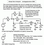
TEXT 368 384 Left 0 !.tran 0 {Td} 10u uic
TEXT 248 320 Left 0 !.param Vdc=0 Vp=1 f1=2k5 f2=250k Td=4m
TEXT 472 -224 Left 0 ;To plot frequency on the\nhorizontal axis change\nthe quantity plotted to\n"V(f)*1Hz/1V" and click\n"Logarithmic"
TEXT 704 -32 Center 0 ;35kHz
TEXT 480 -32 Center 0 ;400kHz
TEXT 64 -336 Left 0 ;This circuit demonstrates the use of a swept sine source to test \nthe large signal frequency response of an idealized UcD180 style \nself oscillatiing class D amplifier, as a function of input amplitude,\ninput offset, and output load.
TEXT 256 232 Left 0 ;Sweep Parameters:\nf1 = start freq f2= stop freq Td = sweep duration\nVp = sine peak Vdc = sine offset
TEXT 408 -392 Center 0 ;Swept Sine Analysis - analogspiceman 2005
TEXT 248 352 Left 0 !.step param Vdc list 0 -4 -8
RECTANGLE Normal 672 -368 144 -416 1
Version 4
SHEET 1 1324 680
WIRE 64 16 64 -64
WIRE 64 128 64 96
WIRE 64 256 64 224
WIRE 64 368 64 336
WIRE 96 -64 64 -64
WIRE 96 224 64 224
WIRE 112 -64 96 -64
WIRE 112 224 96 224
WIRE 224 -64 192 -64
WIRE 224 -64 224 -160
WIRE 240 -160 224 -160
WIRE 256 -64 224 -64
WIRE 256 16 256 -64
WIRE 256 32 256 16
WIRE 256 128 256 96
WIRE 288 -64 256 -64
WIRE 336 -160 320 -160
WIRE 368 16 256 16
WIRE 416 -160 400 -160
WIRE 416 -64 368 -64
WIRE 416 -64 416 -160
WIRE 480 16 432 16
WIRE 544 16 480 16
WIRE 656 16 624 16
WIRE 656 32 656 16
WIRE 656 128 656 96
WIRE 704 16 656 16
WIRE 752 -64 416 -64
WIRE 752 16 704 16
WIRE 752 16 752 -64
WIRE 752 32 752 16
WIRE 752 128 752 112
FLAG 96 -64 i
FLAG 96 224 f
FLAG 64 368 0
FLAG 64 128 0
FLAG 656 128 0
FLAG 752 128 0
FLAG 480 16 x
FLAG 704 16 o
FLAG 256 128 0
SYMBOL bv 64 240 R0
WINDOW 3 -24 168 Left 0
SYMATTR Value V=f1*{f2/f1}**(time/Td)
SYMATTR InstName Bf
SYMBOL bv 64 0 R0
WINDOW 3 -24 168 Left 0
WINDOW 123 -66 214 Left 0
SYMATTR Value V=Vdc+Vp*sin({2*pi*Td/ln(f2/f1)*f1}*{f2/f1}**(time/Td))
SYMATTR InstName Bi
SYMBOL ind 528 32 R270
WINDOW 0 32 56 VTop 0
WINDOW 3 5 56 VBottom 0
SYMATTR InstName Lo
SYMATTR Value 30µ
SYMATTR SpiceLine Rser=10m Rpar=10k
SYMBOL cap 640 32 R0
SYMATTR InstName Co
SYMATTR Value 680n
SYMBOL res 736 16 R0
SYMATTR InstName Ro
SYMATTR Value 6
SYMBOL res 208 -80 R90
WINDOW 0 0 56 VBottom 0
WINDOW 3 32 56 VTop 0
SYMATTR InstName R2
SYMATTR Value 1k8
SYMBOL res 384 -80 R90
WINDOW 0 0 56 VBottom 0
WINDOW 3 32 56 VTop 0
SYMATTR InstName R1
SYMATTR Value 8k2
SYMBOL res 336 -176 R90
WINDOW 0 0 56 VBottom 0
WINDOW 3 32 56 VTop 0
SYMATTR InstName R3
SYMATTR Value 1k0
SYMBOL cap 400 -176 R90
WINDOW 0 0 32 VBottom 0
WINDOW 3 32 32 VTop 0
SYMATTR InstName C1
SYMATTR Value 150p
SYMBOL cap 240 32 R0
SYMATTR InstName C2
SYMATTR Value 33p
SYMBOL Digital\\inv 368 -48 R0
WINDOW 3 0 112 Left 0
WINDOW 123 0 144 Left 0
WINDOW 39 0 176 Left 0
SYMATTR Value tripdt=1n td=200n
SYMATTR Value2 Cout=33n Rout=10m
SYMATTR SpiceLine Vhigh=45 Vlow=-45
SYMATTR InstName A2
TEXT 368 384 Left 0 !.tran 0 {Td} 10u uic
TEXT 248 320 Left 0 !.param Vdc=0 Vp=1 f1=2k5 f2=250k Td=4m
TEXT 472 -224 Left 0 ;To plot frequency on the\nhorizontal axis change\nthe quantity plotted to\n"V(f)*1Hz/1V" and click\n"Logarithmic"
TEXT 704 -32 Center 0 ;35kHz
TEXT 480 -32 Center 0 ;400kHz
TEXT 64 -336 Left 0 ;This circuit demonstrates the use of a swept sine source to test \nthe large signal frequency response of an idealized UcD180 style \nself oscillatiing class D amplifier, as a function of input amplitude,\ninput offset, and output load.
TEXT 256 232 Left 0 ;Sweep Parameters:\nf1 = start freq f2= stop freq Td = sweep duration\nVp = sine peak Vdc = sine offset
TEXT 408 -392 Center 0 ;Swept Sine Analysis - analogspiceman 2005
TEXT 248 352 Left 0 !.step param Vdc list 0 -4 -8
RECTANGLE Normal 672 -368 144 -416 1
Attachments
Hi Analogspiceman,
I'll have to take some time later on and have a really good look at that, but just wanted to say, very nice work and thanks for your continued contributions.
Also I like the look of the idealized circuit. No doubt this will have me spending some quality time with LTspice in the near future.
Thanks,
Chris
Hi Analogspiceman,
I am sorry I can not answer your question about capacitor current feedforward before I become more profficient in LT spice. I tested it with your schematics and I think that I will finally switch from Intusoft Ispice.
I have another question. On Linear Technology download page there is a program called BodeCAD. From what I can see, it takes LTspice schematic and performs series of transient simulations at different input frequencies thus extracting a Bode plot. Has anyone found this program useful?
Best regards,
Jaka Racman
stewin,
I know you are much more experienced as I when it comes to class D, while I was learning the topology I came across one teaching from Hephaestus Audio. This might give you an idea...
Summary of Modulation Schemes
• Self-oscillating
◦ Phase shift or hysteresis
◦ Simple, but may be difficult to synchronize
• Delta-Sigma
◦ Noise shaping pushes noise out of band
◦ High switching frequency lowers efficiency
• Natural PWM
◦ Straightforward, intuitive approach
◦ Easy to synchronize multiple channels
◦ Need to generate high-quality triangle wave
The original document was in pdf (lost the bookmarked link overtime) i do think Delta-Sigma was the more later implementation. It is clear that each modulation scheme has pros & cons. I do hope that a much more in depth analysis from our co-members will enlighten us.
Regards!
Leapfrog Control
Hello analogspiceman,
I am curious about Leapfrog control:
Would it be correct to say that the leapfrog control is sensing load current. So effectively it is making the load current proportional to variations in input signal only and ignoring load impedance variations. Thus making this complete topology as a current driver!?
I hope that you will find time to reply to this one.
Thanks in advance!!
Just to get things started, here is the schematic of a UcD180 power circuit modified to implement leapfrog control (short circuit protection is an inherent, seamless side benefit of leapfrog control). I've also included a very simple, but effective mosfet dv/dt control circuit.
As near as I can tell, LF may be tuned to achieve equal performance to the normal UcD control method, or (unlike UcD) it can be tuned to damp out L-C filter ringing during transient overdrive conditions (where the UcD's feedback loop is momentarily disconnected).
More to follow....
Hello analogspiceman,
I am curious about Leapfrog control:
Would it be correct to say that the leapfrog control is sensing load current. So effectively it is making the load current proportional to variations in input signal only and ignoring load impedance variations. Thus making this complete topology as a current driver!?
I hope that you will find time to reply to this one.
Thanks in advance!!
Leapfrog Control
Hello Pafi,
Thanks for jumping in.
For the same input, the filter inductor current will change with speaker impedance. So if the inductor current is sensed and fed back, we have some sort of current regulation making the circuit a voltage input current output type.
The other feedback is the regular voltage feedback.
I am referring to the diagram in post 9 of this thread.
The leapfrog control I know senses filter inductor current, but not only. An other feedback comes from capacitor also, and the goal of control is output voltage. No difference in this aspect.
As i know,from analogspiceman model it sense resistive current from supply rails to get triangle to get self oscillation and voltage output to get error feedback of sonic. CMIIW.
- Status
- This old topic is closed. If you want to reopen this topic, contact a moderator using the "Report Post" button.
- Home
- Amplifiers
- Class D
- Class d control methods: UcD / LF