Hi
I just make a simple class D amp.
But their is always an offset voltage(7V) at output A and output B.
This make me sad.
What way can I eliminate this offset?
Or...may be my design is wrong?
Or ...need make a change on any part of the circuit
thanks
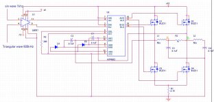
schematic attached
****two waveforms at output A,B ********
I just make a simple class D amp.
But their is always an offset voltage(7V) at output A and output B.
This make me sad.
What way can I eliminate this offset?
Or...may be my design is wrong?
Or ...need make a change on any part of the circuit
thanks
schematic attached
****two waveforms at output A,B ********
An externally hosted image should be here but it was not working when we last tested it.
An externally hosted image should be here but it was not working when we last tested it.
Attachments
Hi,
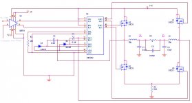
I think you're design is a little off.
L1 and C3 is a filter for one half of the bridge, and connected properly. Then you've got your load connected from that, directly to the other side of the bridge, and there's your mistake.
R3, your load, should instead connect to the node in between L2 and C4, this way it is filtered from both sides of the bridge.
Good luck,
Chris
Apart from the mistake in the output filter in the circuit, this offset is perfectly normal due to the single-ended supply. The important thing is that there is no offset BETWEEN the two output pins. With a full bridge setup, neither output will be zero.
Cheers
Graeme
Cheers
Graeme
Ah yes that's a good point.
However it could all be referenced to a negative rail instead of ground, which would put the outputs near ground potential instead vsupply/2.
I think this method is prefered for safety reasons, the outputs don't sit at a high voltage. Other than that though either way works.
Regards
However it could all be referenced to a negative rail instead of ground, which would put the outputs near ground potential instead vsupply/2.
I think this method is prefered for safety reasons, the outputs don't sit at a high voltage. Other than that though either way works.
Regards
Hi Chris,
Your idea would complicate control circuit a bit. With zero signal, both lower fets should be on all the time. With input signal, one leg would stay on all the time while on the other duty cycle of lower fet would be decreased from 100% to 0%. This would require two PWM comparators and offseting ramp or reference signal for each one. The main problem I see is crossover distortion at small input signals if run open loop.
But there are some designs using above control metod in PFC circuits, where you can get rid of input bridge rectifier.
Best regards,
Jaka Racman
Hi,
as you were told before, your signals look like they should. It is perfectly normal that they operate like that. All full bridge designs do the same. Why do you consider offset to be the problem?
Best regards,
Jaka Racman
as you were told before, your signals look like they should. It is perfectly normal that they operate like that. All full bridge designs do the same. Why do you consider offset to be the problem?
Best regards,
Jaka Racman
Hi Peter_ma, I was wondering what the DC potential between your speaker terminals is. The best way I know to eliminate the chance of it is feedback referenced to a fixed point between power supply rails.
And I am wondering if there is a little bit of DC on the speaker is is such a thing readily or practically addressable, feedback or not.
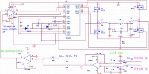
During testing, I choose that circuit (picture)as feedback
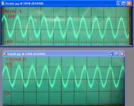
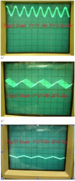
Figure (1) is shown the waveform at (C) when only a diff amp was connected to A and B.(EA ,comarator were disconnected, signals provided function gen.)
After, EA and Comparator were added.
Fig(2) is shown the waveform at negative input of EA.
Fig(3) is shown the negative input at comparatorLM361.
Both fig(2)&(3) were failed to get the proper input to LM361 which need +/- 5V input signal applied.
I replaced R15 with 1.5K but the negative input at LM361 nearly the same as Fig(3). The DC offset was still around -8V. The sin wave always seem disappeared.
I am quite confused.
What is the principle of feedback using diff amp (why need do that way? I build this feedback just by reading information searching from webs and old posts and some hand calculations ¡Kbut I still cannot really understand ¡K )
Also what is the role of EA in this case? What should be possible correct signal at negative input of EA?
More important¡K
Subwo1 mentioned that ¡§The best way I know to eliminate the chance of it is feedback referenced to a fixed point between power supply rails.¡¨
In both fig(2)(3), there always a dc offset. I am afraid ..How the feedback cirucit can eliminate the dc offset?
How can I change the circuit(feedback, ..,even power stage)?
Thanks...all experts
Attachments
You should measure the offset between A and B. As already mentioned, with a single rail you will of course have a DC offset. Ideally it should be 6V with 12V rails, but you haven't added a "virtual" ground that would serve as a reference point.
It could be achieved by biasing the +input of U9B to +6V and feeding the input signal via a capacitor, maybe.
It could be achieved by biasing the +input of U9B to +6V and feeding the input signal via a capacitor, maybe.
- Status
- Not open for further replies.
- Home
- Amplifiers
- Class D
- How eliminate offset voltage in my design