The FQP46N15 MOSFETs are superior to the NTP32N15 ones, I think. What I meant is that if two amps are supplied by a single supply or a +/- dual supply, and the input, stereo or mono, to one them is inverted in respect to the other, the bass reproduction of the two amps will draw power through MOSFETs on both rails simultaneously so long as the inputs have not been independently tone-altered in the bass region of the audio spectrum. The output is put back in phase simply by reversing the speaker connections from one amp. Charles has mentioned this method in the past.
Besides, the logical thing is that overvoltage should have lead to failure of both modules, right?
Not necessarily since one FET might fail at some Volts lower than the other one.
But the fact that your caps come after the fuses rules the supply pumping (for being the cause) out to almost 100 %.
Regards
Charles
Thanks, subwo1. I knew what you meant. But no, there was no pumping compensation at the moment of the failure.
Charles, you are right. Sorry if I insist too much, but I don't think that the supplies have increased more than 45V unless it is too fast that I can't see it with a several ms/div scale. (that's not the nature of pumping, anyway)
Assuming that the rails are +/45V, the mosfets have Vds(br)=150V and that there is no supply pumping, is avalanche still a possibility?
Pierre
You're welcome, Pierre. It seems not to be from pumping. I think it could be from two MOSFETs in a totem being gate-enhanced at the same time. I see two possible causes of that scenario. One is that the Miller effect is turning one back on because its drain voltage rise has exceeded allowable limits. The way to prevent failure from this problem usually involves slower or delayed turn-on of the opposite MOSFET until the first can get itself off and the voltage flown back by the inductor to the opposite power supply rail.
Another is that your MOSFET drive is being triggered spuriously or randomly a minimum of one time, since once is enough to cause cross-conduction, we know. I wonder what other possible causes of the failure there are. I probably left out something.
Another is that your MOSFET drive is being triggered spuriously or randomly a minimum of one time, since once is enough to cause cross-conduction, we know. I wonder what other possible causes of the failure there are. I probably left out something.
Perhaps when connecting inductive loads (i.e. speakers), the PWM waveform has higher spikes at turn off, and it eventually reaches an unallowable Vds value? That could cause one mosfet to fail to shortcircuit due to avalanche, so in the next cycle the other fails too due to overcurrent.
Next time I connect the speakers I will check that waveform and compare it with the resistive load case (where almost no overshoot was found).
If there is another waveform that could be useful to measure, please tell me, I will be doing tests this weekend hopefully.
Pierre
Next time I connect the speakers I will check that waveform and compare it with the resistive load case (where almost no overshoot was found).
If there is another waveform that could be useful to measure, please tell me, I will be doing tests this weekend hopefully.
Pierre
Hi Pierre, I once seemed to attribute to the inductance of the speaker more villainy than it deserved as far as hardship on the MOSFETs themselves. I think now that, generally, its impedance is too high at the switching frequency to put too much relative strain on them. It may contribute to power supply pumping some, though it doesn't seem to affect even that nearly as much as the filter inductor. But it is good you were able to rule out power supply pumping.
In the vein of the two other ideas I mentioned before, I think there could be a chance that at near maximum duty cycle, one MOSFET could be conducting nearly all the time. But when it switches off, it sends the diode on the opposite rail into freewheel conduction. But before that diode's MOSFET gate enhancement delay times out, the lower MOSFET turns back on again before the diode has time to recover. This explanation reminds me of one analogspiceman gave in the past. The question seems to be then, was the output at or near clipping at the time of failure?
In the vein of the two other ideas I mentioned before, I think there could be a chance that at near maximum duty cycle, one MOSFET could be conducting nearly all the time. But when it switches off, it sends the diode on the opposite rail into freewheel conduction. But before that diode's MOSFET gate enhancement delay times out, the lower MOSFET turns back on again before the diode has time to recover. This explanation reminds me of one analogspiceman gave in the past. The question seems to be then, was the output at or near clipping at the time of failure?
It failed while playing music, but it was not clipping I think.
However, how can that be corrected if it is the cause, adding more dead-time?
Your explanation about speaker inductance seems sensible: although it can make things very bad if the loop is not properly compensated, it shouldn't do harm to the PWM waveform itself.
Thanks!
However, how can that be corrected if it is the cause, adding more dead-time?
Your explanation about speaker inductance seems sensible: although it can make things very bad if the loop is not properly compensated, it shouldn't do harm to the PWM waveform itself.
Thanks!
You're welcome. Since the top MOSFET gate charging process aborts in this scenario before it gets beyond V(th), if the deadtime were increased more time would be given for the freewheeling diode to start tapering off its conduction. However this option may not be optional since it can increase distortion greatly.
A better alternative may be to limit the input to the amp to keep the duty cycle from getting too close to 100%. If it were simply limited to 98%, there should be enough time for the associated MOSFET to begin conduction and short the voltage across the body diode. Preventing the amp from clipping prevents the filter resonance from making an appearance and adding to distortion, which is related to control loop retaining its effectiveness along the lines of your comment.
Chris mentioned a possibly ideal way which I think is hard to actually implement. It is to prevent the freewheel diodes from conducting by having the timing of MOSFETs precise enough to avoid the body diodes from ever forward biasing. This way would give the minimum distortion too. But this way would seem very hard for the DIYer to implement, but I suspect that the Hypex UcD amps achieve it.
One thing in your favor which should thwart one of the potential appearances of one of the three cross-conduction failure modes, namely the second one, is that the IR2110 has internal logic which prevents both outputs from being driven on simultaneously. That feature is one that I like about the chip. I blew plenty of MOSFETs from that occurrence before I found the IR chip.
It is to prevent the freewheel diodes from conducting
This can also be done using a technique developed by Brian Attwood. He constructed the output coil as an auto-transformer that feeds two fast-recovery diodes so that the body diodes never get into conduction state.
Regards
Charles
Hi Pierre,
I would try increased "dead time" via a bigger gate resistor, if you have ten ohms there now, try it with 20, and maybe even up to 50, in increments.
That should help you rule out the body diode as a possible problem area.
I know it will switch slower but, if you use an old IRF640 it will very likely last the long haul, providing the cooling is there for it. It's harder to drive and will switch alot sloppier all around, as well as the higher Ron.
You may find this interesting, but I've run them in a circuit for days at rather high temps, and they toughed it out for awhile. The circuit had errors which led to serious shoot through. In that same circuit I tried the same mosfets you mentioned that are found in the UCD400. They lasted all of thirty seconds. Seems the more optimal the device is the more optimal everything else has to be as well.
I have the circuit largely fixed now and it has played for a few days with what I think just may be even more optimal devices, the lower mosfet is rather warm but not hot, the upper mosfet is actually cold, I blame a few causes but for the purposes of that particular implementation, it's good enough.
So I feel you're probably better off with a bigger turn on resistor and a more optimal mosfet, than trying to get a dino of a fet to switch fast and efficiently. That's not at all to say not to try the 640 though, go for it.
I think you may have just tried to get the optimal value for THD and in doing so crossed that fine line, and an extra few ohms might be enough to save it.
The other odd thing discussed before is the regenerative effect which causes the upper mosfet to snap on quicker. Does the bottom mosfet run hotter than the top? You could possibly try only increasing the turn on resistor for the upper fet on it's own, and see what smokes. I think trial and error is the way to go because what are the odds you'll catch the very instant on a scope??
You could actually also try a different mosfet in the bottom than on top. I think a slightly slower device on top and a more Cdv/dt immune fet on the bottom. Once you have the problem all narrowed down you might have a tenth look at your layout with that in mind, not to say I know of any problem with it, but maybe you'll spot something you dont' like when you have a better idea of eactly what you're looking for.
Best of luck, I'm looking forward to when you have it all figured out.
Regards,
Chris
Thanks for all your support.
I will try with two identical circuits but different mosfets:
FQP46N15's in one and IRF640N's in the other. Let's see which of them lasts more time in the same conditions. However, at the end, I would like to go for a lower Rds(on) for efficiency. I really don't know why FQP46N15 shouldn't be perfect!
classdforsure: I really didn't notice which of the mosfets was hottest, because they are now placed "back to back" in a common heatsink.
Charles and subwo1: I am sure that techniques are quite optimal, but I am also sure that the circuit can work perfect in terms of reliability while keeping it this simple. For example, IRF ref. design uses a very similar power stage, Crest LT also does, there are plenty of designs using the basic app. note of the IR2110 devices. I think it is "only" a matter of having the right mosfets, the right layout and the right dead-time and turn on/off times.
BTW: Anyone knows what mosfet the current ZAP Pulse modules have?
Best regards,
Pierre
One thing more, to clarify things:
After reading the philips App.note on avalanche SOA:
It seems to me that repetitive avalanche failure should be produced by either exceeded repetitive avalanche energy or by exceded junction temperature over a long time. My mosfets weren't too hot, so _if avalanche was the problem_, the avalanche energy rating must have been exceeded.
To sumarize, the single-pulse avalanche energy is:
Eas=0.5 x L x Ias^2 x (Vbr/Vbr-Vcc)
being Vcc the total rails voltage and Ias the inductor maximum current (Vout_max / RL_min)
Is this correct? That gives about 3mJ, much less than rating.
BUT: How is repetitive avalanche energy calculated?
Thanks!
Hi,
You can try lets say a 3 to 1 ratio turn on / turn off resistor value.
This way you have a moderate turn on (10-20 Ohm) and a fast turn off (2.2-4.7 Ohm).
Layout is crucial, no load current shall pass the drivepath and the
path (drive-return) shall be as short and low in inductance as possible.
Otherwise the driver can't hold the gate down. Also look at the ratio of the Miller vs gate source cap. If the gs cap is lower than the
miller add a few nF to gs to split the miller charge kicking back.
The IR drivers can output anything and also break if the Vs node
goes south of com by more than a few volts.
/ Mattias
Thanks, Mattias.
Is the Miller cap Coss (output capacitance) or Crss (reverse transfer capacitance)? I suppose it is Crss.
In the FQP46N15, Ciss (input capacitance) is 2500pF typ, while Crss and Coss are 100 and 520pF respectively.
In the NTP35N15 the relationship is very similar.
For the control of turn on/off times, I currently use a 10r resistor in parallel with a schottky, so turn on has the 10r gate resistor while turn off is done as fast as the driver can.
What do you think?
Thanks
Ah, about miller charge (Qgd), it is about double of Qgs charge, but this happens in FQP46N15, NTP35N15 and even in IRF640N, which ZAP pulse amps used. Is that what you were referring to?
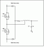
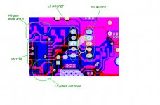
My layout is not bat IMHO. The gate signals are only crossed by heavy current tracks in the yellow marked zones of this scheme:
Hope this drawing is clear enough to follow the gate drive routing. Mosfets are mounted "back to back".
Thanks.
My layout is not bat IMHO. The gate signals are only crossed by heavy current tracks in the yellow marked zones of this scheme:
Hope this drawing is clear enough to follow the gate drive routing. Mosfets are mounted "back to back".
Thanks.
Attachments
Boy that's a can 'o worms.
The gate charge ratio topic isn't a straight forward one and if you do some searching you'll find many conflicting app notes on the topic.
First the repetitive avalanche question, the two links I gave on the topic explain it and give some examples, I think you have to make use of the thermal impedance curves...
Back to the gate charge ratio:
Even some mosfet manufacturers actually make claims of Cdv/dt
"immune" parts and all they use is the ciss/crss ratio outright, which doesn't seem right because it's alot more complex than that. I'm stunned they make semiconductors and prescribe to that theory.
Here's a fine example:
http://www.semtech.com/pdf/sc420.pdf around page 8. It even recommends adding that gate to source capacitor.
I personally don't feel the gate to source capacitor would be an effective counter measure, It would "split" the miller charge only after it's acted upon the gate by passing through the gate resistance, so it wouldn't help the problem at hand, and also slow turn on. It may however allow the gate to sit lower with respect to the source and by doing so make it a little more immune to gate step, but that's ugly, as a diagnosis measure you wouldn't know if it is helping make it more immune to the gate step by having the gate go lower, of it if helping by slowing Dv/dt. I'd just go with trying a bigger resistor and seeing what happens.
Here's the app note I go by:
http://www.irf.com/technical-info/whitepaper/syncbuckturnon.pdf
Use a spreadsheet to make a calculator based on Eq:12 and you can compare mosfets with one another alot more quickly. Is it 100% bullet proof method? Apparently not, but it gives you some idea and is alot more accurate than just ciss/crss which is unrealistically simple.
I'm no PCB artist but those current loops don't look all that short? I think you really want all the parts kissing, or as close to that as you possibly can.
Best Regards,
Chris
Wow! That appnote is very good!
I am starting to think that my problem is not mosfet rudgeness but Cdv/dt turn on or spurious turn on due to couplings in the gate drive paths.
Does this problem (Cdv/dt) apply only to the lower mosfet or it does to both of them?
I will look at this appnote more deeply and also at my waveforms on saturday.
Thanks for your help.
I suspect that Qgd or Qgs1 are not directly that especified in the datasheets as "Qgd" and "Qgs", right?
In that case, one must calculate the correct Cgd and Cgs values (not readily available in the datasheets) from the other C's given, right? And that depend on the Vds voltage.
For example, IRF640 datasheet says:
Ciss=Cgs+Cgd, Cds shorted
Crss=Cgd (wow! we have one)
Coss=Cgd+Cds.
So we have Cgd=Crss and Cgs=Ciss-Cgd?
Then, from datasheet's fig.5: for this mosfet at Vds=100V: Cgd=Crss=300pF
Cgs=Ciss-Cgd=1500pF-300pF=1200pF
Thus Cgd/Cgs=0.25 (OK)
For NTP35N15:
Cgd=Crss=nearly 0pF
Cgs=Ciss-Cgd=2200pF aprox
Thus Cgd/Cgs is very low (OK)
Is all this well done?
Nope, but your close.
You're strictly using capacitance and you need to evaluate it using charges.
I'll quote the app note:
"However, Cdv/dt induced
turn-on at Q2 also depends on Vds and threshold voltage
Vth. It then makes sense to use gate charges instead of
gate capacitances to evaluate the Q2 device.
One intuitive way of interpreting the Cdv/dt induced
turn-on problem is the accumulated miller charge. When
Vds reaches the input voltage, it should be smaller than the
total charge on Cgs at the Vth level so that Q2 will not be
spuriously turned on."
Use equation 12 found on page 5. That's why I mentioned a calculator might make it easier to compare different mosfets quicker. But yeah, you do need to read the capacitances like you had done, and plug those into the equation.
I tried explaining it before as I understood it:
http://www.diyaudio.com/forums/showthread.php?postid=433641#post433641
I think you'll find the answers to be less optimistic.
- Status
- This old topic is closed. If you want to reopen this topic, contact a moderator using the "Report Post" button.
- Home
- Amplifiers
- Class D
- Mosfet reliability in Class D amplifiers