Yes, they are both n channel mosfets. I am reversing the design now and hand write the schematic.
The v- mosfet is drived by one of the two schmit trigger chip, and is referenced to v- , no to ground, while the v+ mosfet is drived by the other chip, referenced to ground then.
Maybe one of the flaw in the design?
Happy new year John !
The v- mosfet is drived by one of the two schmit trigger chip, and is referenced to v- , no to ground, while the v+ mosfet is drived by the other chip, referenced to ground then.
Maybe one of the flaw in the design?
Happy new year John !
Happy new years guys.
Have a look at the supply line for the upper schmitt IC "driver" see if it's powered by a bootstrap cap/diode circuit. One thing I read about as well is caps going bad on these... maybe that's the one? Seems off for that to go but.... hey *shrug*. Sounds like reaaally weak drivers anyway.
I'm also surprised it's only a half bridge, if it is harris, all their patents I've seen seemed to use a full bridge. Maybe you can take the IC's off and test them in a dumby circuit for basic operation or something.
Cheers
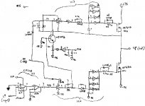
Ok, here is my first drawing, duno if it is 100% acurate. It seems that there is a boostrap to power up the upper 74, with c5 and the diode on its right.
maybe i have done mistake while reversing it, but it seems quite simple.
Any tought???
thanks and a happy new year to every one !!!
maybe i have done mistake while reversing it, but it seems quite simple.
Any tought???
thanks and a happy new year to every one !!!
Attachments
Ok, after some testing on my bredboard, the schmitt trigger chip for the v- mosfet is shot, toasted, dead.  All other components test good, even if they look burned (because of the way i have removed the epoxy, with a flame torch
  ).
).
Looking at the schematic, there is not protection diode on its vcc line, while the upper one, got one. You should see a zener diode at the right of c5 rather than a plain diode.
The vcc for this is issued from the bridge rectified -95v, with some diodes and 3x 10k resistor in parralel, making a -89v if measured from the ground. This chip (IC2) is referenced to the -95v, so it got +6v at its vcc.
I will build a prototype with better voltage limitations/protections for both chips, with more caps for filtering, there is very few of them, actualy only 0,1uf.
The opamp is also very badly powered. It is by the means of 3x 4.7kohm resistor in parralel, 2w, and a 15 volt zener diode, same circuit for the +vcc and -vcc, making a poors man +15 0 -15. Source is directly from the bridge rectified +95v and -95v There is no decent caps on this too, only a 100nf on the main board of the whole unit. what a sh*t.
Sorry for my poor schematic, i will do a better one with my cad (power logic) when i will go back to work.
All other components test good, even if they look burned (because of the way i have removed the epoxy, with a flame torch ).Looking at the schematic, there is not protection diode on its vcc line, while the upper one, got one. You should see a zener diode at the right of c5 rather than a plain diode.
The vcc for this is issued from the bridge rectified -95v, with some diodes and 3x 10k resistor in parralel, making a -89v if measured from the ground. This chip (IC2) is referenced to the -95v, so it got +6v at its vcc.
I will build a prototype with better voltage limitations/protections for both chips, with more caps for filtering, there is very few of them, actualy only 0,1uf.
The opamp is also very badly powered. It is by the means of 3x 4.7kohm resistor in parralel, 2w, and a 15 volt zener diode, same circuit for the +vcc and -vcc, making a poors man +15 0 -15. Source is directly from the bridge rectified +95v and -95v
There is no decent caps on this too, only a 100nf on the main board of the whole unit. what a sh*t. Sorry for my poor schematic, i will do a better one with my cad (power logic) when i will go back to work.
Hi, nicely done I'm impressed!
I think I see the basics on how it's trying to work. Simple for sure.
Few things I'm unsure of.
After the bootstrap circuit, there's a diode, a 5kR, then an inverter, the positive supply of that inverter looks like it's connecting to to all that, is that the case? AAAAhhh, the 5kR must be a collector load. I bet that diode must be a 12V zener.
I'm not seeing anything that would charge that bootstrap cap on power up.. but I see you have a bit of a line/something drawn up above that doesn't seem to go anywhere, are we missing anything from this?
What connects to that... inverter? that goes to the BJT's emiter? Not the feedback point?.... I can't figure that part out at all, but I don't see any other place for a feedback input, John?")
IRF640's... switching pigs. You can certainly improve on that choice.
I have a feeling there's an error in those "driver" voltages.
Being N channels you have to bring gate +~12 with respect to source to switch on, it looks like the ground is wired to -95+12, it would always be on and couldn't turn off like that.
All the rest seems like it could make sense to me
Regards and Happy New Year
I think I see the basics on how it's trying to work. Simple for sure.
Few things I'm unsure of.
After the bootstrap circuit, there's a diode, a 5kR, then an inverter, the positive supply of that inverter looks like it's connecting to to all that, is that the case? AAAAhhh, the 5kR must be a collector load. I bet that diode must be a 12V zener.
I'm not seeing anything that would charge that bootstrap cap on power up.. but I see you have a bit of a line/something drawn up above that doesn't seem to go anywhere, are we missing anything from this?
What connects to that... inverter? that goes to the BJT's emiter? Not the feedback point?.... I can't figure that part out at all, but I don't see any other place for a feedback input, John?
IRF640's... switching pigs. You can certainly improve on that choice.
I have a feeling there's an error in those "driver" voltages.
Being N channels you have to bring gate +~12 with respect to source to switch on, it looks like the ground is wired to -95+12, it would always be on and couldn't turn off like that.
All the rest seems like it could make sense to me
Regards and Happy New Year
You were posting while I was writing.
Nice work you're on the ball! Don't need my 2cents but I cant' stop myself, nothing on TV.
So what do you suppose that inverter off the BJT is for? I can take a few guesses but.... nah, not at this hour.
I knew something was fishy with those voltages. 6V was my first guess but it didn't make sense so I kept looking at it, hard to make out the writing too. I would think that would have burnt the mosfet out before the inverter though, not turning it fully on. If the driver is burnt, the mosfet must be, are you positive it's OK? Burnt mosfet would go along way to explain that loud hum you had too. Wow, how'd they let it go out the door like that? Something to be said for DIY alright.
There needs to be some type of means to charge that bootstrap cap on power up too, with a delay, you already have the zener there, you just need two more resistors, one from positive rail to one side of the zener and one from the other side of the zener to the negative rail (thanks John), maybe you have a delay with it already too? You dont' really need another zener on the lower one, not if say it were comming off a 12V linear regulator IC.. or any "decent" regulated supply of some sort, which it sounds like you'll be adding.
Maybe since you're redoing it you'll consider using a decent gate driver IC, but if that worked with those mosfets, adding decent mosfets for switching should be enough of an improvement to let you sleep at night.
This was fun, thanks!
 funny, yet, not really.
Right out of no where, dawns the light.
That inverter on the bjt+diode... start delay / precharge. Seems you knew that "SD" Start delay.. You know what that's the coolest part of the whole amp!
Anyway, you seriously did an excellent job reversing this thing, and in no time at all.
So, is there no feedback on this thing?
Hi Pat & Chris,
Well done in tracing the circuit so quickly.
The modulator circuit doesn’t make much sense – where’s the oscillation element? I would have expected to at least see a feedback path from the OPS to the first integrator via the integrator Cap or a resistor… If the Cap was connected from the OPS then it would look a little like UCD / hysteresis switcher…
A Single ended Sub amp – now that’s just asking for trouble! - now I wonder why the PSU caps are so big
John
Ok, i have tripple cheked the boostrap circuit, i did a litle mistake, the zener is on the right side of the 5k resistor, not directly in parallel with c5.
D6 might be responsible of some sorf of initial start?
The RF connector on the top left corner is connected to nothing on the pcb, but is there.
i am not that much familiar with class D amps, but i see the main thinking behind it all.
What surprises me is the total absence of active protection, wathever is happening, full dc voltage will go thru the woofer.
Yes, i am 100% sure of that, both mosfets are ok.
On the main board, there is a feedback resistor from input to output. 56.2k.
SD is some sort of protection where it stops the unit to oscillate, but isnt there somethin wrong with this, one of the 2 mosfet will stay on then?
On the other schematic i have (original PB12 power amp module version 2), they show a lot more filtration caps for the opamp, and the IR2111 driver, so they knew it was a flaw in the design .
There is a relay and a temperature sensing on the "better" circuit. Maybe i will inspire myself in doing my protoype
Thanks for all the good comments.
Good morning,
MM.. coffee good.
Ok, D6 that's the bootstrap diode? Yeah it kind of is responsible for precharge in the sense that it is in the precharge path.... if I'm right about this that is.
I'm not 100% sure on this, but on power up SD is probably brought high, which brings node/pin 8 low on the inverter, creating enough of a drop to forward bias the diode, turning on the BJT and pulling down to the negative rail, once that is done it charges up the bootstrap cap to... 6volts through D6.
When SD is brought low, node 8 goes high, forces the diode into blocking mode /disabling the precharge circuit and then the bootstrap cap is ready to "fly" all charged up.
Standby mode must just hold SD high keeping it in precharge mode as well. The only way I can see it keeping the lower driver disabled is by syphoning off current through the base to prevent the lower driver from being driven, maybe this explains the use use of that 1K resistor in the lower driver path, limit the current to the base so this balancing act can work. That's just alot of speculating though, thoughts?
So I guess that 5K is doubling as both a current limiter for the zener and acting as a pull up for the collector.
Can you find out what the zener voltage is? At this point I'm getting curious as to wether or not they used 6volts drive voltage intentionally to help tame the switching behavior of the mosfets, I'm shocked that they weren't burnt, impressive, I still think they're pigs though, they have a fairly high Ron too.
Thanks
MM.. coffee good.
Ok, D6 that's the bootstrap diode? Yeah it kind of is responsible for precharge in the sense that it is in the precharge path.... if I'm right about this that is.
I'm not 100% sure on this, but on power up SD is probably brought high, which brings node/pin 8 low on the inverter, creating enough of a drop to forward bias the diode, turning on the BJT and pulling down to the negative rail, once that is done it charges up the bootstrap cap to... 6volts
through D6. When SD is brought low, node 8 goes high, forces the diode into blocking mode /disabling the precharge circuit and then the bootstrap cap is ready to "fly" all charged up.
Standby mode must just hold SD high keeping it in precharge mode as well. The only way I can see it keeping the lower driver disabled is by syphoning off current through the base to prevent the lower driver from being driven, maybe this explains the use use of that 1K resistor in the lower driver path, limit the current to the base so this balancing act can work. That's just alot of speculating though, thoughts?
So I guess that 5K is doubling as both a current limiter for the zener and acting as a pull up for the collector.
Can you find out what the zener voltage is? At this point I'm getting curious as to wether or not they used 6volts drive voltage intentionally to help tame the switching behavior of the mosfets, I'm shocked that they weren't burnt, impressive, I still think they're pigs though, they have a fairly high Ron too.
Thanks
That amp is modified by a owner for sure, that would explain the big ps caps, about the oscillator element, it could be self oscillating or the oscillator was on the main board. With a voltage at 95 volts per rail the current is so low that the transformer doesent need to be any larger.
Hi,
I doubt it was modified, it was encased, Pat had to cut open the case and chisel out the epoxy. There seems to be have been several revisions of it at factory + the amp module changed entirely though, so there's alot of variations of it floating out there I'm sure. (Both amp module versions eventually were cancelled due to the all the problems they've had with them).
The big PSU caps, well, it is a half bridge sub woofer, small caps at low frequency on a half bridge would pump up pretty good I think.
It havent been modified, the big caps were added by the company that did service it first time, it is part of a recal in the service manual.
SD seems to be always high, it is pumped externaly by a zener diode (1n5265b, 6.8v) and a 8.2mohm resistor, making some soft start because of the high r value, and the C11 that could be around 0,47uf. The short circuit protection that is on the main board will put SD low (-95) if activated there is 3x 0,1ohm resistor on the ground path of the speaker output, wich will activate a pair of transistor to activate another one, and then put SD low, in case of a short at the output, maybe it limits the overall power output?
I am slowly understanding every components, i have also measure some caps and resistors to complete the schematic, the only 2 missing are the C1 cap on the first op amp, and the cap above the 1k resistor marked with a ? C9 is 47p.
SD seems to be always high, it is pumped externaly by a zener diode (1n5265b, 6.8v) and a 8.2mohm resistor, making some soft start because of the high r value, and the C11 that could be around 0,47uf. The short circuit protection that is on the main board will put SD low (-95) if activated
there is 3x 0,1ohm resistor on the ground path of the speaker output, wich will activate a pair of transistor to activate another one, and then put SD low, in case of a short at the output, maybe it limits the overall power output?I am slowly understanding every components, i have also measure some caps and resistors to complete the schematic, the only 2 missing are the C1 cap on the first op amp, and the cap above the 1k resistor marked with a ? C9 is 47p.
So they must have been suffering from supply pumping and blowing up supply caps. That's consistent with some posts I've read too about blown supply caps, and they just fixed it by adding bigger caps, which is fine.
Is there a chance that circuitry on the output is just there to sense current flowing, so that it knows it is oscillating and disables the pre charge circuit? You don't need it once it is oscillating as it refreshes the cap with each cycle.
I just dont' see how that bjt can disable this thing. I'd have to simulate it, but thankfully, that's your job
I was going to simulate this thing, but....  Maybe I will
Anyway, no wonder it smoked, can't believe it ever worked at all, whoever "designed" this was dancing on the razors edge blindfolded and loving it.
Your schmitt trigger hex inverter, you said was MC74ACT14AN, don't know what that last "A" is for.. , it is part of the "ACT" cmos family, advanced cmos, TTL compatible inputs.
Characteristics of this family, Vcc MAX=5.5!
They were running with >6, and unregulated.
Also, you're just not switching an IRF640 fully on with 6volts gate drive, they must have run hot.
Options:
You could use a 10V cmos inverter, but that would be much slower (1 or 2Mhz as opposed to the 100Mhz the ACT family is good for) and the threshold will be alot higher, around 5 volts I think, might not work very well.
Or, could possibly add some type of follower or other gate driver, extra parts, extra supplies, complication..yuck.
My idea: rebuild as is, but fix the supplies like you planned, regulated to 5.1 volts, and use a logic level mosfet.
Check this one out:
At Vgs=10, Rdson=.075 Ohms
At Vgs=4.5, Rdson=.08 Ohms
Vth min = 1volt
Vth max=2volts
http://www.fairchildsemi.com/pf/FQ/FQA34N20L.html
I think that'd be a big improvement, with no added complication or significant redesign.
Maybe I will Anyway, no wonder it smoked, can't believe it ever worked at all, whoever "designed" this was dancing on the razors edge blindfolded and loving it.
Your schmitt trigger hex inverter, you said was MC74ACT14AN, don't know what that last "A" is for.. , it is part of the "ACT" cmos family, advanced cmos, TTL compatible inputs.
Characteristics of this family, Vcc MAX=5.5!
They were running with >6, and unregulated.
Also, you're just not switching an IRF640 fully on with 6volts gate drive, they must have run hot.
Options:
You could use a 10V cmos inverter, but that would be much slower (1 or 2Mhz as opposed to the 100Mhz the ACT family is good for) and the threshold will be alot higher, around 5 volts I think, might not work very well.
Or, could possibly add some type of follower or other gate driver, extra parts, extra supplies, complication..yuck.
My idea: rebuild as is, but fix the supplies like you planned, regulated to 5.1 volts, and use a logic level mosfet.
Check this one out:
At Vgs=10, Rdson=.075 Ohms
At Vgs=4.5, Rdson=.08 Ohms
Vth min = 1volt
Vth max=2volts
http://www.fairchildsemi.com/pf/FQ/FQA34N20L.html
I think that'd be a big improvement, with no added complication or significant redesign.
- Home
- Amplifiers
- Class D
- JBL PB12 subwoofer, Class D amp, dead.