As an experimenter with Class-D amplifiers, I have found that it is not easy to properly design the feedback network when you want to include the LC output filter on it, and make the amp remain estable.
I think that some designs (self-osc or UCD) use positive or "hysteretical" feedback, but I am not interested on that, but on designing the compensation network for a basic PWM (triangle based) amplifier with negative feedback, including a single LC network (2nd order lowpass).
I have seen that there is a so-called "leapfrog" method, but I am not able to extract the phisical sense and design procedure for that case from the PDF. Are there some basic guidelines or simple explanations?
Phase_accurate, I have seen you are kind of an expert in these issues, can you help me, please?
Thanks!
Salut Pierre
Sorry for not responding earlier. I have been on holiday. In the meantime also my hotmail account was erased due to not using it.
If you have e-mailed me you message might have got lost.
There are many ways to build the triangle-based modulator itself. Could you tell us something about the ciscuit decisions that you have made so far ? Are you willing to share the final design ? If so I am of couse willing to assist.
Regards
Charles
Thanks for the help offering and don't worry for the delay, Charles.
My set-up is, by the moment, a simple experiment:
An error opamp configured as inverting amplifier, the signal enters via a resistor to the inv. input. The output goes to a comparator, and the other input of the comparator receives the triangle.
The output filter values are 20uH and 440nF.
What I would like is to include a 2nd order filter (LC) into the loop so the output impedance is reduced and the freq. response is made almost independent on the load, and the overall response is similar to a 1st order lowpass, while reducing distortion due to non-linearities of the ouput filter.
If you could give general design guidelines on how to design the feedback network to compensate for the filter phase shift, I think it could be very useful for any Class-D amp designer.
thanks!
Before we try to close the loop around everything: Does everything look fine open-loop. I.e. no ringing on the switching signal (with and without load) ?
How does it look like if you close the loop around the the switching stage (what this topology is meant to be used like) ?
If everything is working fine so far (important, if you don't want to do annoying debugging) we need to know the component values of your integrator and the gain of the switching stage (basically the PSU/trinangle-amplitude voltage-ratio).
Then we are able to rearrange the loop filter to take the output filter into consideration.
Regards
Charles
Thanks for your help, Charles.
Well, by now I have a 68k resistor between mosfet's output , with input resistor to the error opamp of 2k. (looking for a 30dB gain).
The output stage gain is 15, aprox. (6Vpp triangle with +/-45v supply rails).
The error opamp (integrator) capacitor is 470pF, and a 100K resistor in parallel, to improve DC offset, etc.
Now the loop is closed aroung switching stage. With this setup and a 10ohm in series with 330n zobel network, the -speaker- output has ringing only with light loads (above 20 ohms or so), overshoot for 8 ohms and very clean below that.
Is this a good start point?
With this setup and a 10ohm in series with 330n zobel network, the -speaker- output has ringing only with light loads (above 20 ohms or so), overshoot for 8 ohms and very clean below that.
What I meant was the PWM signal itself. Things like ringing etc can lead to interesting effects like increased THD when the loop is closed (instead of the contrary). The output-signal of the comparator must also look clean, without glitches etc, since this can lead to premature death of mosfet-drivers.
One important thing I forgot to ask: What is your carrier frequency ?
And another point: We are free to change the actual closed-loop cutoff frequency within some limits. Do you want to do this ?
Regards
Charles
Ah, ok.
The PWM signal looks very good. The rise and fall times are about 70ns and there is almost no overshoot. So does the comparator output.
About the operating frequency, I feel comfortable with 260-300KHz, although I can vary this. (after all, this is an experiment!)
About the cutoff frequency, I would like to have about 30KHz at -3dB for 2ohm to 8ohm loads.
What do you think about my Zobel network? In my simulations it actually helps damping things when there is no load.
If I have time I will try to post some photos of the PWM and play a bit with the feedback network so I can give more details. My primary concern when closing the loop around filter is estability.
Thanks, Charles, for helping us in demystifying the "feedback after filter" problem!
What do you think about my Zobel network? In my simulations it actually helps damping things when there is no load.
I also think that it is a good idea to use it but I would maybe lower the capacitor's value. One critical situation with after-filter NFB takeoff is the no-load situation. Though it might not be as severe in practice as in simulations, since practical filter parts are always lossy. But it would be a good idea to switch the thing on for the first time (i.e. the first time using after-filter NFB when it worked beforehand using before-filter NFB) WITH a resistive load connected.
As a start I would use the following:
1.) A 47 pF cap in parallel with your 68 k feedback resistor. This gives a phase-lead in the closed-loop and determines the overall upper cutoff-frequency.
2.) Decrease the Integrator cap to 330 pF since this will give you more NFB. With this value there is still some marging, so you won't get into problems when lowering the carrier-frequency below 260 kHz.
3.) Use a resistor of 10 k in series with said integrator cap. This will make your integrator (actually a PT1) into a PI. The FR of this "turns flat" at the output-filter pole frequency at said dimensioning.
4.) Play around with the integrator's parallel resistor. A larger one will lead to more NFB and lower THD at low frequencies. Smaller values however will lead to a more constant NFB factor throughout the audio range (and therefore more constant THD behaviour over the input- frequency) and faster overload recovery. Your 100 k is about the largest I would recommend. Maybe you will try with 47 k as an alternative.
You might actually try it first on the simulator.
And one more thing: Have fun !
Regards
Charles
Thanks!
It's funny! Just this afternoon I was playing with the simulator a little bit. Although my model doesn't include the switching nature of the amplifier (it is just an opamp -the integrator- , then a linear gain -the switching stage gain-, and then the filter), I hope the results can be extrapolated.
Before reading this, I have tried by adding a 82pF capacitor in parallel with the 68k resistor, and it has solved almost all the problems. I haven't currently added 10k in series with the integrator cap, but I will try your suggestion to see its effect. I had also lowered the 100k to 47k and I now I like it more.
Let's see if I can try this in real life as soon as possible, and let's see also if the pulse response is as good as in the simulation, as well as the freq. response, that has become almost load independent!
Thank you very much for your help. Should I find any more optimizations, I will publish them here, no doubt.
I think that these guidelines can help a lot of Class-D designers.
Cheers
Hi, Charles.
I added a resistor in series with the integrator cap as you suggested, and now the simulated freq. response is better (no ringing) with no load, so it does improve things.
A last question before putting hands into the lab: how can I measure phase margin in the simulation? Sorry, but I have forgotten the details since I studied it, so if you want to remind me... can I measure it in open loop or is it necessary to introduce an excitation while maintaining it close-loop, as it is done when designing power supplies compensation?
What is a good phase margin figure for these kind of amps?
If you are so kind to explain the procedure I (and many others) would be very pleased.
Thanks!
Phase marging can be measured (i.e. simulated) by opening the NFB loop, grounding the input and feeding the signal into the feedback branch.
If you then simulate the frequency response and display it as phase and gain plot, you can look at the phase of the output signal at the unity-gain point (you can of course also measure it on the real amp that way). The phase-difference between the actual output signal and 180 degrees is the phase-marging. One is trying to have more than 90 degrees, but this would be in a perfect world, in reality it is usually less. Even many excellent-sounding linear amps out there have only about 45 degrees !!! But values between 60 and 90 degrees can be achieved with properly designed switching amps.
Regards
Charles
Wow, that's a fast response!
So, in an inverting setup like mine and many others, that means that I should break the loop by disconnecting the output from the feedback network, and then insert a test voltage in the feedback input (where before was the output), then ground the input, and compara the output with the test signal, that is?
Thanks!
Well, there's where my small mess comes: if the setup I have explained before is correct, the simulator gives a DC shift of +180 degrees (that's logical, it's inverting), and a DC gain of about 23dB.
Phase is going down until it is +77 degrees where the gain is 0dB.
What is the phase margin there?
My reasoning is this: Gain should be less than 0dB when phase is 0 degrees, so the output has gone round from +180 degrees to 0 degrees and hence it is in phase (oscillation occurs), so phase shift in my case is 77 degrees (in the simulation, of course ;-)
That's with 8 ohm load. The funny thing is that with 2 ohms load, the phase at 0dB is +105degs. That is too good. Am I doing something really bad?
Cheers.
Ouch !!
I made a mess myself. Since you already have 180 degrees by the inversion (that is actually necessary for NFB) it is the difference to 360 degrees (where oscillation would start to occur) that is relevant. So you have 77 degrees now which is quite cool !
If you load your filter more heavily two things happen: It is damped more and its phase-change gets less steep. Secondly the amplitude response is also less steep with an earlier rolloff. Both these things together may get you the effect you described. The unity-gain frequency will not be the same again however (from a first guess it is lower now), but who bothers as long as the overall outcome is a stable frequency response for all load conditions ?!
Regards
Charles
Well, if I reduce it to 4.7k then it crosses 0dB at 110KHz (4 ohm load), so ok.
Please, could you explain why did you wanted that condition? And how did you do the calculations? (if you are willing, of course ;-) I did some drawings and inserted the zero to lead phase shift and compensate the loop, but these subtle details escape to my (present) knowledge.
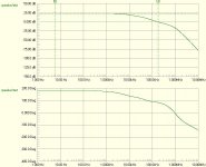
This figure is the speaker vs input freq. response at 4 ohms. It looks almost exactly the same for other loads. Do you think that the strange phase / gain change at about 10 MHz is worrying? I suppose it is due to the hf pole of the opamp.
Thanks.
Please, could you explain why did you wanted that condition? And how did you do the calculations? (if you are willing, of course ;-) I did some drawings and inserted the zero to lead phase shift and compensate the loop, but these subtle details escape to my (present) knowledge.
This figure is the speaker vs input freq. response at 4 ohms. It looks almost exactly the same for other loads. Do you think that the strange phase / gain change at about 10 MHz is worrying? I suppose it is due to the hf pole of the opamp.
Thanks.
Attachments
Please, could you explain why did you wanted that condition?
Because a class-d amp is a discrete-time control system the loop gain has to be lower than unity at the Nyqvist frequency. IMHO the assumption that the Nyqvist frequency is half the carrier frequency (that many sources mention) is not completely valid, since we make two decisions per carrier cycle. As long as there is no drive signal the Nyqvist frequency (i.e. half the rate at which decisions are taken) is the same as the switching signal. With increasing modulation index, the two instances where decisions are taken, move closer together until they happen at the same time for 100% (or 0 % ) duty-cycle and is therefor reduced to the switching frequency. The only practical solution to expliot this fact is a self oscillating class-d amp (at least to my knowledge).
The only case when the values can be simply and elegantly determined mathematically is the case with an output filter with a Q of 0.5 but this is not very practical.
So the only values that were actually exactly determined is the integrator C and the parrallel capacitor for the feedback branch.
As soon as I have time and I am motivated enough I will put it on paper (er word document) and post it here.
Regards
Charles
Edit: I wouldn't worry about the phase-change at 10 MHz.
Well, I am very happy with the results of the simulations. Let's see if they reproduce as well in the reality. At least I (and I am sure that many more people) have gained a little bit of "sensibility" on the issue.
Let's see if I can post some related useful schematics or oscilloscope images when the measurements are done.
Thanks, Charles, sincerely.
Let's see if I can post some related useful schematics or oscilloscope images when the measurements are done.
Thanks, Charles, sincerely.
Well, now some real-world results:
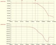
I have implemented the changes in one of my prototypes (although the coil is 33uH and the cap is 1uF instead of 20uH+440n, so they are not identical to the simulations conditions).
The system works quite well, with very good transient (square wave) response (check the image: no overshoot and fast response). The gain and bandwidth are as expected also.
However, I have found slightly more distortion with a sine wave input than before, when the feedback was taken before the filter. Check the image.
On the other hand, the waveform doesn't degrade with high power levels. In fact, the image shows 72Vpp on 5 ohms, but it was the same with 70Vpp at 2.65ohm (230W rms). It is present in the whole audio band.
I think I should try with more feedback, perhaps reducing the 68k resistor (and recalculate the comp. capacitor in parallel accordingly). Do you have any suggestions?
Thanks!
Attachments
- Status
- This old topic is closed. If you want to reopen this topic, contact a moderator using the "Report Post" button.
- Home
- Amplifiers
- Class D
- Help with feedback