Hi Bruno,
Are you an LTspice user? It works better than Pspice (IMO) and is a free download from the software page of the Linear Technology web site.
The simulation file I posted in the other thread uses averaged models for the switching stages, so it runs like lightning. The line current envelope is visibly modulated by the low frequency audio output, although this effect is lessened by the two pole low pass filter on the current feed forward.
If you haven't done so already, you ought to give LTspice a go with the pfc sim file from the other thread. It's fun.
Regards -- analog(spiceman)
Note: this post copied from the UcD180 thread for continuity
I've been playing with an LTspice simulation of a 180 W UcD style class d amplifier with a power factor corrected power supply (with and without voltage balancing on the outputs). The pfc front end has been set up with a voltage loop crossover frequency of 17 Hz (with a second pole at 16 Hz), a 16 Hz double pole low pass filter on the rectified ac feedforward squared divisor signal, and a 10 Hz double pole low pass
filter on the output current feedforward multiplier signal. Override operating limits are 4 amps on the input current and 400 volts on the output voltage. AC input range for proper operation is 80 to 264 volts
and nominal dc output is 375 volts. A 330uF capacitor is used for primary energy storage.
The pfc front end is followed by a simple dc to dc step-down supply for the isolated rail voltages. Its step-down ratio is 0.12, yielding a nominal 45 volts or so for the class d rails. A 10,000uF capacitor is
hung on each rail so that total output energy storage is just slightly less than that on the 330uF boost capacitor. The rail voltages are balanced by an auxiliary circuit that can easily be disconnected by
setting its series resistance to a high value.
The output load is my guess at an equivalent RLC network for a nominal 4 ohm woofer with a 34 Hz box resonance. For the test run shown, the amp is overdriven with a 15 Hz clipped sinewave burst. Without active balancing the positive rail voltage gets pumped up to a whopping 59 volts at the end of the burst. With the balancing circuit in place it remains safely well under 50 volts at all times.
An interesting note about the voltage balancing circuit: by designing it with a certain controlled level of impedance, it can avoid having to handle the large reactive currents required to keep the two output
capacitors in lock step, yet still nicely squelch the pumping effect. (I intend to cover my ideas on balancing circuits in another post.)
The LTspice simulation file is attached, but I had to change the file extension to from ".asc" to ".txt" in order to get it to post (you'll need to change it back after downloading).
Regards -- analog(spiceman)
Bruno Putzeys said:
On the face of it, "getting an SMPS to work" may be simpler than UcD (as the large amount of working power supplies of various quality shows), making a really good SMPS is not to be sneezed at.
Off the shelf (OTS) SMPS's tend to have the following failings:
All methods necessary to make good SMPS's are known and understood, but only by a small number of experts (I have good reasons to believe analogspiceman is one of them). Unfortunately, these true experts number hardly more than the number of class D experts. Until one of these few takes time out to do something special for audio, we're still better off using linear supplies.
- Maximum peak power = average power
A 100W power amp draws 200W peaks. An OTS supply will therefore have to be selected for 200W. Of course it'll be overrated then, too large and too expensive. I'm unaware of SMPS's where thermal design and regulation (sagging instead of cutting out) are optimized for audio use. As a result, using a standard SMPS will make your product lighter but much bigger than a 50 Hz transformer!- Terrible EMI. The layout quality standard of most SMPS's is years behind on that used by seasoned class D designers.
- Ridiculously large Y caps between primary and secondary (made necessary by incorrect choice of transformer form factor and pinout).
- PFC, if present, overshoots at around 17 Hz (current feedforward never heard of, although many of these controller chips have dedicated input pins for this)
I am personally trying to find time to make such a "good smps", more specifically a single stage PFC+galvanic isolation, the aim being to put the storage on the secondary side, get high efficiency, good pfc but only basic regulation.
Unfortunately my experience with high-voltage (primary side) design is not very great so a product won't be ready anytime soon. In the meantime - all eyes on analogspiceman
I've been playing with an LTspice simulation of a 180 W UcD style class d amplifier with a power factor corrected power supply (with and without voltage balancing on the outputs). The pfc front end has been set up with a voltage loop crossover frequency of 17 Hz (with a second pole at 16 Hz), a 16 Hz double pole low pass filter on the rectified ac feedforward squared divisor signal, and a 10 Hz double pole low pass
filter on the output current feedforward multiplier signal. Override operating limits are 4 amps on the input current and 400 volts on the output voltage. AC input range for proper operation is 80 to 264 volts
and nominal dc output is 375 volts. A 330uF capacitor is used for primary energy storage.
The pfc front end is followed by a simple dc to dc step-down supply for the isolated rail voltages. Its step-down ratio is 0.12, yielding a nominal 45 volts or so for the class d rails. A 10,000uF capacitor is
hung on each rail so that total output energy storage is just slightly less than that on the 330uF boost capacitor. The rail voltages are balanced by an auxiliary circuit that can easily be disconnected by
setting its series resistance to a high value.
The output load is my guess at an equivalent RLC network for a nominal 4 ohm woofer with a 34 Hz box resonance. For the test run shown, the amp is overdriven with a 15 Hz clipped sinewave burst. Without active balancing the positive rail voltage gets pumped up to a whopping 59 volts at the end of the burst.
With the balancing circuit in place it remains safely well under 50 volts at all times. An interesting note about the voltage balancing circuit: by designing it with a certain controlled level of impedance, it can avoid having to handle the large reactive currents required to keep the two output
capacitors in lock step, yet still nicely squelch the pumping effect. (I intend to cover my ideas on balancing circuits in another post.)
The LTspice simulation file is attached, but I had to change the file extension to from ".asc" to ".txt" in order to get it to post (you'll need to change it back after downloading).
Regards -- analog(spiceman)
Attachments
Here is [the link to] the gif of the simulation:

I just figured out how link to an existing file which avoids wasting storage space on the server to duplications. My apologies to the group and moderators that I didn't think of doing this for the previously attached text file.
  analog(spiceman)
I just figured out how link to an existing file which avoids wasting storage space on the server to duplications. My apologies to the group and moderators
that I didn't think of doing this for the previously attached text file. analog(spiceman)Thanks for starting this thread, Bruno. Now I will take the opportunity to talk about my switching power supply design.
Anyone interested in circuit simplicity may like to investigate the USMPS. I thought of the name before I learned about the existence of the UcD. I like it as well as the UcD because it is composed of simple blocks. The USMPS is easy to modify for almost any application. I use variations of it for most of my power needs. Within the next several months, I plan to update the schematics and files on the Yahoo group I founded. If someone would like to become a group moderator, please contact me. That person should be passionate about the design and willing to promote it freely to all equally. I have no monetary profit motive.
Anyone interested in circuit simplicity may like to investigate the USMPS. I thought of the name before I learned about the existence of the UcD. I like it as well as the UcD because it is composed of simple blocks. The USMPS is easy to modify for almost any application. I use variations of it for most of my power needs. Within the next several months, I plan to update the schematics and files on the Yahoo group I founded. If someone would like to become a group moderator, please contact me. That person should be passionate about the design and willing to promote it freely to all equally. I have no monetary profit motive.
Hi analog,
Seems you're off to a good start!
Modelling a 4ohm woofer as having a 2ohm dc resistance is a bit unrealistic. The definition of "nominal impedance" is that at no point modulus of impedance is to drop more than 20% below this (3.2 ohms). The DC resistance is pretty much on that order.
15 Hz full power is somewhat unusual too, but it's a good acid test considering the loop bw of the PFC. I am under the impression (didn't test this - don't shoot me if I'm wrong) that the modulation is partly exacerbated by the PFC's own overshoot.
Could you add current feedforward to the simulation and check what happens then?
Cheers,
Bruno
From my limited sampling, 3.2 ohms would be about typical with some 4 ohm nominal units weighing in just under 3 ohms at dc. I used 2 ohms in the simulation both because it was a whole number and because then the load's series and parallel losses during the clipped pulse summed almost exactly to 200 watts. Admittedly, this would be kind of an excessive worst case scenario for the UcD180.Bruno Putzeys said:Modelling a 4ohm woofer as having a 2ohm dc resistance is a bit unrealistic. The definition of "nominal impedance" is that at no point modulus of impedance is to drop more than 20% below this (3.2 ohms). The DC resistance is pretty much on that order.
I changed the double pole low pass filter in the current feedforward path from 1Hz to 1kHz and it had almost no effect on the "pumping effect" voltage overshoot at the end of the pulse train. This is also a worst case scenario because the load's inductive current (which is at its peak when the train of clipped sinewaves abruptly ends) has enough time to discharge totally into the positive supply's 10,000uF capacitor, pumping it to the max. Since the output power supply diode is back biased, any small variations in the rise of the pfc boost output play no role here.Bruno Putzeys said:15 Hz full power is somewhat unusual too, but it's a good acid test considering the loop bw of the PFC. I am under the impression (didn't test this - don't shoot me if I'm wrong) that the modulation is partly exacerbated by the PFC's own overshoot.
Could you add current feedforward to the simulation and check what happens then?
By the way, putting too much bandwidth in the current feedforward path most definitely does vastly increase the distortion and flicker in the ac input current waveform.
Regards -- analog(spiceman)
Alternative SMPS Configurations
Hi Guys, and thanks Bruno for starting this thread. I have also been following the UcD thread with great interest.
I think an SMPS for amps is of interest to a lot of people and it is a subject I have spent some time researching myself. The traditional approach to include PFC seems to be the standard PFC boost converter front end followed by some form of switching down converter (half bridge/full bridge, etc).
One possible alternative that I have looked at but is rarely seen commercially is the current fed topology (inductor in the primary line). This may be a push-pull, full bridge, etc and allows the PFC and down conversion to be achieved in a single stage. Because a PFC IC is used in the control loop secondary ripple rejection is low and will be determined by the size of capacitor tank on the secondaries but a large bank is desirable for audio amplifiers particularly in class-d half bridge because of supply pumping. However, although there are large caps in the secondary there aren't in the primary (because of the pfc action).
What this circuit does is achieve output power regulation (albeit with some mains line ripple) over a universal input voltage range and is scalable from small powers to kilowatts where it is most cost effective.
To summarise, the following advantages and disadvantages of this topology are:
Advantages:
PFC and down conversion in a single stage.
Magnetic components approximately the same as the two stage approach. (But still considerably reduced in size over a normal 50Hz supply)
Excellent cross regulation characteristics on multi output supplies because of the single primary inductor current feed with no minimum output current requirements like a normal forward mode PSU.
Secondary regulation across a wide supply input.
No shoot through when configured as a bridge or push pull because of the current fed feature - in fact part of the operation as you store the energy in the inductor is through deliberate overlap.
Disadvantages:
Increased output mains ripple over the 2 stage approach but for an amplifier with normal PSRR this is not a problem.
Slightly increased high frequency output noise but can be oversome with some secondary fillering.
No off the shelf control IC's - but can easily be implemented with a conventional PFC ic with some external logic.
Possibly have to use an active primary clamp depending on design configuration.
Summary:
After doing quite a bit of work on this it looks very attractive for cost effective small size audio supplies with integral PFC, however I have never seen it used commercially. This maybe because of some inherant problems (which I would be interested in comments on) or alternatively because not much has been written about this configuration.
I look forward to some feedback
Robin
Re: Alternative SMPS Configurations
I've finally found a small amount of funding for looking into a single-stage pfc smps, albeit using a somewhat different topology. I have once seen a paper that does what you suggest (if I understand you well). A pair of switches build a pp converter. The switches are made to overlap to charge a coil which is in series with the ct of the primary. There could be a controller IC to do this.
The thing I'm looking at is: replace the diode in the pfc boost converter by a small switch and change the boost cap into a small film thing (now an active clamp). Make the boost coil the primary of a transformer. Rectify the secondary with an inductor-input fw rectifier.
The voltage on the active clamp cap is a measure of the secondary voltage so that can be used as a feedback takeoff point.
Performance is identical to a two stage converter.
I can start this thing end of november. I'll keep you posted.
Alternative Configurations
Hi Bruno,
Your understanding of the topology I proposed is correct. You can also use a bridge instead of the p-p (even a zero voltage switched full bridge).
The topology you propose is very interesting. However, it sounds like you would still need a forward inductor for each output so I guess you would still have minimum load concerns at low currents for multiple outputs without some clever mutual windings. I understand that you will be able to achieve better secondary regulation with a faster dynaic response but I was particularly interested in multiple output supplies in which case the current fed converter behaves very much like a normal multi tapped transformer except with the addition of pfc and regulation against changes in line input voltage.
It is at last refreshing to discuss some of these topologies with someone who has an open mind and the knowledge to consider something different to the norm. You would not believe the number of psu designers that look at you with a blank face if you propose anything that isn't a normal forward or flyback converter")
Robin
Hi Bruno,
Your understanding of the topology I proposed is correct. You can also use a bridge instead of the p-p (even a zero voltage switched full bridge).
The topology you propose is very interesting. However, it sounds like you would still need a forward inductor for each output so I guess you would still have minimum load concerns at low currents for multiple outputs without some clever mutual windings. I understand that you will be able to achieve better secondary regulation with a faster dynaic response but I was particularly interested in multiple output supplies in which case the current fed converter behaves very much like a normal multi tapped transformer except with the addition of pfc and regulation against changes in line input voltage.
It is at last refreshing to discuss some of these topologies with someone who has an open mind and the knowledge to consider something different to the norm. You would not believe the number of psu designers that look at you with a blank face if you propose anything that isn't a normal forward or flyback converter
Robin
Hi Robin,
have you considered what happens in current fed topology when reflected secondary voltage is below peak of the line voltage? IMHO this topology only works in boost mode.
Bruno,
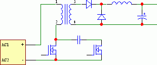
is this roughly what are you considering? Do you intend to achieve continious input current with this configuration?
Best regards,
Jaka Racman
edit: after rereading Bruno's post, I think there is a mistake in the rectifier configuration in my schematic. But the question about continious input current still remains.
have you considered what happens in current fed topology when reflected secondary voltage is below peak of the line voltage? IMHO this topology only works in boost mode.
Bruno,
is this roughly what are you considering? Do you intend to achieve continious input current with this configuration?
Best regards,
Jaka Racman
edit: after rereading Bruno's post, I think there is a mistake in the rectifier configuration in my schematic. But the question about continious input current still remains.
Attachments
Hi Jaka,
Absolutely correct, this topology does work in boost mode as a normal pfc front end would, the difference being that the power switch configuration is different to allow both control of the pfc loop as well as the modulation for controlling the output voltage through a transformer.
Robin
Absolutely correct, this topology does work in boost mode as a normal pfc front end would, the difference being that the power switch configuration is different to allow both control of the pfc loop as well as the modulation for controlling the output voltage through a transformer.
Robin
Hi Robin,
my main concern is the startup transient. I once considered this kind of topology for charging a rather large bank of capacitors (several kJ of stored energy) and found no simple way to control inrush current when reflected secondary voltage was below peak of the mains voltage.
Best regards,
Jaka Racman
Hi Jaka,
By using a kind of active clamp on the primary after the inductor and across the transformer and power switch you can get it to operate in flyback mode during startup and fault conditions which controls this phenomenon until the output voltage reaches it's normal level. I worked the required logic out once driven from a pfc ic. I'll have to try and dig it out to post for you.
During normal operation the active clamp then acts to aid zero voltage switching across the bridge as well as act as a clamp.
I hope all this makes sense.
Robin
Following what I mentioned earlier, until I dig out some of my old material on this, have a look at this datasheet for a unitrode device (TI). Although this device is now discontinued it shows the idea of a current fed topology and the logic is not at all hard to work out. I, in fact worked on a slightly different configuration but this is nevertheless interesting.
www.bmh.nu/pdf/Switch/UCC3857.pdf
Robin
www.bmh.nu/pdf/Switch/UCC3857.pdf
Robin
Hi Robin,
makes perfect sense, thank you.
Here is my opinion about various topopogies in SMPS. In spite of myriad of topologies, you can not bend the laws of physics. There is no transformer isolated topology that can process the same amount of power as non isolated one with switch element of the same rating. Because you have to maintain volt seconds balance on the transformer, you either have to use single switch with higher voltage rating or two or more switches with the same voltage rating. I have seen many articles proposing various single switch PFC topologies, but the added complexity usually results in the same amount of components as the two stage approach.
My choice for amplifier power supply would be probably simple self oscillating flyback, maybe even with bipolar transistor instead of mosfet. I would not care about PFC, if it is not specifically required for audio. PFC does not solve flicker problem, which may also be problematic with non class A audio amplifiers.
BTW, does any one know what are current agency regulations regarding audio amplifiers? Are they considered class1( protectively earthed) or class2 (double isolated) equipment. How is output handled where it can exceed Extra Safe Low Voltage? What about DC protection at the output? I have a friend that had an accident with his amplifier. Because of cold solder joint on amplifier PCB, DC offset literary burned one of the loudspeakers down. Fire has caught woofer membrane and then grille cloth. If he was not at home, his house would have burned down.
Best regards,
Jaka Racman
Hi Jaka,
Barring the rectifier, your schematic reflects what I'm up to, except that in my drawing the clamp switch and cap are swapped so you get a ground-referred feedback takeoff point.
The input needs a filter, since the primary current is not a neat triangle.
I do intend to achieve zvs on both switches.
Cheers,
Bruno
Re: Alternative Configurations
It's most easily solved by converting to synchronous rectification, but that would undo the principal aim, which was simplicity. On the upside, it would automatically couple the rails, completely ridding us of the class d psu pumping problem that folks are making such a lot of.
Well as I might have said this is pretty much my first smps project... let's see where it goes.
Dammit you're right...Robin said:However, it sounds like you would still need a forward inductor for each output so I guess you would still have minimum load concerns at low currents for multiple outputs without some clever mutual windings.
It's most easily solved by converting to synchronous rectification, but that would undo the principal aim, which was simplicity. On the upside, it would automatically couple the rails, completely ridding us of the class d psu pumping problem that folks are making such a lot of.
Well as I might have said this is pretty much my first smps project... let's see where it goes.
Hi Jaka.
I'll check on the class I/II thing and let you know. Regarding the output voltage of the amplifier, higher power amplifiers are indeed considered a hazard and as such they changed the spec for agency approvals in europe on the speaker connectors. Old style binding posts were not allowed to have exposed contacts anymore which meant the all metal type could not be used and even the plastic ones had to have exposed parts shrouded. What people did to get round this was plug the end cap where you would insert a banana plug with a plastic bung that was easily removed so that if someone took it out to use banana plugs they did it at their own risk....
I don't think DC protection is mandatory and it is really at the discretion of the manufacturer. Lower power amps generally never have and some higher power amps do. In professional audio I would say that most quality amplifiers have DC protection but in hifi many manufacturers don't seem to bother. There is always the problem of how you tackle it without putting something nasty in the audio path (typically a relay at the amplifier output). I have seen other schemes that crowbar the supply fuses or trip out a relay in the mains feed that forms part of the soft start. Using an SMPS actually simplifies this as it is easy to shut down the supply without having to put extra components in the audio path
- Status
- This old topic is closed. If you want to reopen this topic, contact a moderator using the "Report Post" button.
- Home
- Amplifiers
- Class D
- SMPS design for power amps (Class D in particular)