Hi everyone,
Excellent driver cookbook you have there Eva. Thank you for sharing it, I'm sure it can serve for class D designs as well, it shows some good techniques. Clearly you know what you're doing.
Nice scope, sure wish I had one like it.
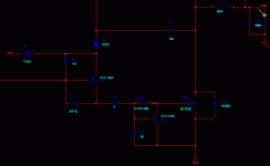
Here is one driver leg of the UCD circuit....I would have included more...but it would be soooooo small you woulnd't see anything...so this will just have to do.
This seems to switch ok...(I'll give you a sample next post). With these resistor values, rise and fall times of the driver transistor match those of the data sheet.
Seeing how tempermental this circuit is to even the slightest changes, I'm having my doubts about prototyping it without a scope. See what happens...I'm not afraid of a little smoke.
Thanks,
Chris
Excellent driver cookbook you have there Eva. Thank you for sharing it, I'm sure it can serve for class D designs as well, it shows some good techniques. Clearly you know what you're doing.
Nice scope, sure wish I had one like it.
Here is one driver leg of the UCD circuit....I would have included more...but it would be soooooo small you woulnd't see anything...so this will just have to do.
This seems to switch ok...(I'll give you a sample next post). With these resistor values, rise and fall times of the driver transistor match those of the data sheet.
Seeing how tempermental this circuit is to even the slightest changes, I'm having my doubts about prototyping it without a scope. See what happens...I'm not afraid of a little smoke.
Thanks,
Chris
Attachments
Hi,
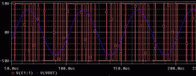
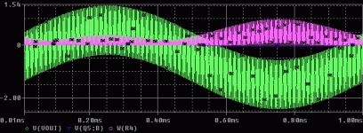
This is the output at the half bridge, before and after the coil.
Input is 2V AC at 20Khz to make it easy to see. This also clearly shows the next problem I need to work out with it, I think it stems from some sort of imbalance at the input stage that I haven't been able to nail down yet.
Thanks,
Chris
Attachments
Hi,
Pafi, you're welcome, but thank Bruno, it's his design")
It's not really a new problem I've just ignored it until now.
When I run THD simulations it tells me "DC component -0.5" or so.
If you look very carefully at the last graph I posted, the PWM wave amplitude sags with the inverse of the input signal amplitude. This happens at all frequencies and input levels that it accepts (100mV to 2 volts AC).
So I guess basically the output rides on an inverse portion of the input. I've tried to match currents through the input stage as closely as I can, and the closer they get the better it gets, but it's still there, and I haven't been able to diminish this by more than .5 volts, even with the comparators currents matched down to the milli-amp range.
With a lower powered version of this exact circuit, the best I've had was THD .2% at 1Khz and 1 volt input.
With the higher powered version I just posted, I get about 6%. This is with no extra low pass filtering of the output.
So it still needs lots of work, but it's comming along.
Btw, the driver transistors I'm using were calculated at 550 ohms...which works but it's ugly. 110 Ohms seems ideal.
If anyone else is working on this I'd love to hear about it.
Thanks,
Chris
Pafi, you're welcome, but thank Bruno, it's his design
It's not really a new problem I've just ignored it until now.
When I run THD simulations it tells me "DC component -0.5" or so.
If you look very carefully at the last graph I posted, the PWM wave amplitude sags with the inverse of the input signal amplitude. This happens at all frequencies and input levels that it accepts (100mV to 2 volts AC).
So I guess basically the output rides on an inverse portion of the input. I've tried to match currents through the input stage as closely as I can, and the closer they get the better it gets, but it's still there, and I haven't been able to diminish this by more than .5 volts, even with the comparators currents matched down to the milli-amp range.
With a lower powered version of this exact circuit, the best I've had was THD .2% at 1Khz and 1 volt input.
With the higher powered version I just posted, I get about 6%. This is with no extra low pass filtering of the output.
So it still needs lots of work, but it's comming along.
Btw, the driver transistors I'm using were calculated at 550 ohms...which works but it's ugly. 110 Ohms seems ideal.
If anyone else is working on this I'd love to hear about it.
Thanks,
Chris
Hi,
Pafi,
Just had a chance to check these out. The IRFB31N20D looks alot like the IRFP250 at a glance, you'd think twins. I don't have a model for it though.
The W34NB20, oddly I could find no information on at all.
The FDP2552 looks very promissing, I just might try that model in fact. Is 150volts drain -source a big enough margin of safety for +-50 volt rails?
The two I could find information on look like excellent candidates anyway, thanks for sugesting them.
Had I tripped over that last one sooner my circuit would look different now.
Any comments on my choices of diodes?
Thanks,
Chris
Pafi,
- Maybe you should choose faster MOSFET. For example IRFB31N20D, W34NB20, or under 150V: FDP2552...
Just had a chance to check these out. The IRFB31N20D looks alot like the IRFP250 at a glance, you'd think twins. I don't have a model for it though.
The W34NB20, oddly I could find no information on at all.
The FDP2552 looks very promissing, I just might try that model in fact. Is 150volts drain -source a big enough margin of safety for +-50 volt rails?
The two I could find information on look like excellent candidates anyway, thanks for sugesting them.
Had I tripped over that last one sooner my circuit would look different now.
Any comments on my choices of diodes?
Thanks,
Chris
Chris!
I mean thank you for the link!
DC similarity is intentionally, but I tryed to find faster, and lower Qg FETs!
+/-50 V is OK, but because of supply pumping you must watch the supply, and turn off the amplifier, if goes too high! With bridged amp there is not a problem like this. (I use +/-70V supply with FDP2552).
Diodes: in driver they seem to be OK, but the 1N4003 on output I don't see any denefit on them. You'd better to use a MOSFET with faster dody-diode! The mentioned FDP2552 is excellent, since its Qrr is only 300 nC! APT makes amazing MOSFETs too. (For example 20M36BFLL.) Buy from them if you can!
W34NB20 is made by ST, search at www.st.com!
P.S.: Be careful! IRFP250, and IRFP250N are not the same! 250N is superior in speed!
Hi,
Pafi, I'm seriously impressed...you're like a walking mosfet inventory
I didn't even know about the IRFP250N, I don't have a model of it though.
It seems I would be foolish not to go with the FDP2552...I ...feel it...beckoning me...pulling me in..closer....
I'm still pretty far from the point where I have to worry about supply pumping, but you are of course correct.
Thanks,
Chris
Hi Chris and everyone else,
To my experience you can't beat a driver IC. Although EVA showed that
it is possible to do with discretes.
When driving large die FETs at high speed the losses in the drivers will
be significant and to my believe it is hard to find discrete components
that can be fast enough and have the dissipation you need.
Also, the layout is hard to keep tight even with the ICs.
Regarding the tailing effects maybe some volts negative drive at turn off
may improve. I have never used that on FETs however and don't know
if it takes the tail off.
Last, I get inspired by your courage. No scope doing switch-stuff, thats brave!
At home I have some old Philips and TEK but they don't do much good either.
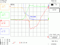
I append a scope-shot from a dc/dc using Warp 2 IGBTs and IR2113s driver that shows
some tailing effect for thoose that have not seen this live.
The IGBTs are thrown out now.
/ Regards Mattias
To my experience you can't beat a driver IC. Although EVA showed that
it is possible to do with discretes.
When driving large die FETs at high speed the losses in the drivers will
be significant and to my believe it is hard to find discrete components
that can be fast enough and have the dissipation you need.
Also, the layout is hard to keep tight even with the ICs.
Regarding the tailing effects maybe some volts negative drive at turn off
may improve. I have never used that on FETs however and don't know
if it takes the tail off.
Last, I get inspired by your courage. No scope doing switch-stuff, thats brave!
At home I have some old Philips and TEK but they don't do much good either.
I append a scope-shot from a dc/dc using Warp 2 IGBTs and IR2113s driver that shows
some tailing effect for thoose that have not seen this live.
The IGBTs are thrown out now.
/ Regards Mattias
Attachments
ekaerin said:Hi Chris and everyone else,
To my experience you can't beat a driver IC. Although EVA showed that
it is possible to do with discretes.
When driving large die FETs at high speed the losses in the drivers will
be significant and to my believe it is hard to find discrete components
that can be fast enough and have the dissipation you need.
Also, the layout is hard to keep tight even with the ICs.
Regarding the tailing effects maybe some volts negative drive at turn off
may improve. I have never used that on FETs however and don't know
if it takes the tail off.
Last, I get inspired by your courage. No scope doing switch-stuff, thats brave!
At home I have some old Philips and TEK but they don't do much good either.
I append a scope-shot from a dc/dc using Warp 2 IGBTs and IR2113s driver that shows
some tailing effect for thoose that have not seen this live.
The IGBTs are thrown out now.
/ Regards Mattias
Hi there,
Do you find your at home scopes too slow? If I did get one it would be have to be the cheapest I can find, but I guess a 1Mhz scope wouldn't cut it would it.
Do those tail currents contribute to "supply pumping"? I just saw a diagram/pic of supply pumping in action and it looks strikingly like what I have going on...which I find curious as I have no capacitors to be pumped as I'm only using a VDC source.
If I waited until I had a scope alot of time would be going down the drain when I could be learning something..
I've gotten alot better with spice lately anyway, learnt alot about driving mosfets, no parts have gone up in smoke..
I have wired a few class D circuits just for kicks, powered them +-12 and 1 amp regulated...Just to see how it sounds.
I found qualities in the sound I liked alot, every note jumps out of the speaker with alot of life and transparancy, I can only dream of having that at 500W, for at the same time, lots of crackle, which is where I leave them at, with no scope handy.
I also shame the designs I test by just grabbing whatever parts I have around...including 741's and "best fit" caps that were cut from an old motherboard or PSU.
Gladly I dont' have these limitations in the land of spice, however it's plagued with it's own.
So as I said, I've learnt alot, it's yet to cost me a dime. I can however assure you, while I'm willing to let the smoke out of the odd component, I will protect my Cerwin Vegas at all cost, I do plan on buying a used scope off of ebay some day, but they are far from cheap aren't they.
Until then, on the brighter side of things, even a black 100 Ohm ...is still 100 Ohms.
Thanks,
Chris
Chris,
The tail was from an IGBT. I have personally never seen it on FETs at least
not to that extent. I dont think the tail will contribute to the pumping of
the supply.
Do you get the pumping in spice with an ideal voltage source ?
On my bench at work I use a LeCroy LT344 waverunner but even that
is to slow when looking at diode recovery. Then I need to use a
4ch 1GHz sample / 2ch 2GHz sample scope to get it nice. But I could also
have used the old analog Tek we used to have. The best thing with the
digital scopes is the wave storage for further analysis.
If you want to get a scope, my personal advice is to go for an old Tectronix scope.
Nowadays people go for digital but the old analog scopes can be really
fast, and probably sheap too. No menus and crap, all is there on the front panel.
But even with the best of scopes, measuring anything switchmode is not
an easy thing to do. You need to be careful where you ground the probes
if you're not using isolated diffprobes. Also, common mode noise to give you
fake ringings etc.
/ Mattias
Hi,
Yeah it really looks like it, sounds silly doesn't it? I woulnd't go so far as to say that's what's causing it yet, so for now I'll blame it on the DC offset which isn't acceptable at .5V. Same sort of effect though.
Chris
Do you get the pumping in spice with an ideal voltage source ?
Yeah it really looks like it, sounds silly doesn't it? I woulnd't go so far as to say that's what's causing it yet, so for now I'll blame it on the DC offset which isn't acceptable at .5V. Same sort of effect though.
Chris
tail in MOSFET
Hi !
I was also not aware of a tail current in MOSFETS.
In EVAs screen shot it would be interesting to see the drain current.
I am not sure if the delayed voltage
of the FET might be caused by some parasitic capacitance.
It might be that the current drops without much delay, but only the voltage swing is delayed.
Of course it is hard to measure fast voltages and currents correctly related.
Normally the current measurement equipment ( current probe + amp) delays the current trace longer than the voltage trace.
This gap can easily be around 100ns ... 200ns, already a long signal
wire between current measurement equipment and scope gives some ns delay.....
And not everyone has a LECROY at home that allows to adjust that timing! (@eakerin: I am trying hard not to get envious )
@ Chris!
Yes, it is a good idea to buy a scope.
Simulation and reality typically do not match perfectly at first approach.
Usually you have measure the real thing and the differences against
the simulation will give you hints about several parasitic effects.
In second step you may try to add these undesired effects to your simulation.
After this the simulation may again help to get rid of such troubles.
Cheers
Markus
Hi !
I was also not aware of a tail current in MOSFETS.
In EVAs screen shot it would be interesting to see the drain current.
I am not sure if the delayed voltage
of the FET might be caused by some parasitic capacitance.
It might be that the current drops without much delay, but only the voltage swing is delayed.
Of course it is hard to measure fast voltages and currents correctly related.
Normally the current measurement equipment ( current probe + amp) delays the current trace longer than the voltage trace.
This gap can easily be around 100ns ... 200ns, already a long signal
wire between current measurement equipment and scope gives some ns delay.....
And not everyone has a LECROY at home that allows to adjust that timing! (@eakerin: I am trying hard not to get envious
)@ Chris!
Yes, it is a good idea to buy a scope.
Simulation and reality typically do not match perfectly at first approach.
Usually you have measure the real thing and the differences against
the simulation will give you hints about several parasitic effects.
In second step you may try to add these undesired effects to your simulation.
After this the simulation may again help to get rid of such troubles.
Cheers
Markus
Marcus and Pafi,
1st. Marcus, I whish I had thoose scopes at home but I have them only
at work.....
2nd. Pafi, I can not show you the schematic. But it is from a DC/DC fullbridge
included in a 3phase input rectifier with true 3phase PFC as input boost.
The DC/DC runs from about 380Vdc from high side to output.
The IGBTs where tested to see if was possible to use them because of
lower cost compared to MOS-FETs. However, dispite theese where the
fastest IGBTs for the application the tailing losses became too much at
high temperatures. So we could not use them more than up to an
ambient temperature of 50C. That was about 140C on the IGBTs case
when runaway started to show up.
The IGBTs wereWarp-2 series IRGP50B60PD1 from International Rectifier.
The device is aimed towards 150kHz and although we used 50kHz we
could not use it in our design. But it is anice device anyway.
/ Regards / Mattias
Pafi,
The scaling, offsets and timing are not perfectly aligned but the traces are:
Ch1: C-E voltage of lower switch
Ch2: C-E voltage of upper switch
Ch3: Current of lower switch (turning on)
Ch4: Current of upper switch (turning off and shows the tail)
The peak current is about 25Ap in each IGBT.
Current probe used is a LeCroy AP015 with a 50:1 ratio small toroid core
around the leg of the transistors. (very cheap but very good)
/ Mattias
Hi everyone,
I haven't been able to improve the DC offset at all, any sugestions? I'm stuck with -0.5 volts on the output. Powering comparator with 40mA and the output resistor Rb is 30 ohms for 20mA output....input is going straight to the base, any sort of grounding scheme (divider...10pF cap...) makes no difference.
Of course it's spice so the transistors are perfectly matched. The diodes that seem to work best for me are 1n914's and transistors are 2n5401 and 2n5551.
The pwm output seems centered about zero until it starts riding on the inverse of the input which looks like power supply pumping, but that can't be it as there isn't one it's just VDC sources, while the sine wave output is what has the -.5 dc offset.
Any ideas would be well appreciated.
Thanks,
Chris
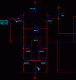
Hi,
Comparator circuit with output wave, input was 50mV 1khz. Even the graph of power over the load is riding an offset which I seriously don't understand, could this be a spice failure? I'll demonstrate more clearly what I mean by that in the third pic.
Thanks,
Chris
PS: I'll try to squeeze in the full circuit as well
Attachments
- Status
- This old topic is closed. If you want to reopen this topic, contact a moderator using the "Report Post" button.
- Home
- Amplifiers
- Class D
- poor switching