....looks fine.....
But please note that you should modify for this
simulation value of Ron for the Sbreak in the "breakout.lib"
Normally Ron is set to 1 Ohm. You should change it to
0.005 Ohms which reflects the RDS_ON of the paralleled FETs.
How to change? Depends on you PSpice/ORCAD version.
One method always works.
Open the breakout.lib with any text editor and search for the
Ron....... change.... save..... done.
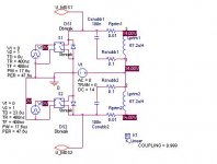
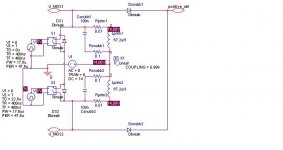
For real live the snubbers should be placed close to the windings
of the transformer. Also the current load for the snubber cap
may be fairly high. I placed the resistor in series to snubber cap only in order to damp RF-ringing. From simple theory it would be allowed to make it 0 Ohms.
But it must be low value. Because the leakage inductance will press
very high currents through the snubber. If resistance is to high, then the snubber cannot protect the MOSFETs at high load conditions....
The first pic is the primary.... had to split primary and secondary because of the allowe pic size.
But please note that you should modify for this
simulation value of Ron for the Sbreak in the "breakout.lib"
Normally Ron is set to 1 Ohm. You should change it to
0.005 Ohms which reflects the RDS_ON of the paralleled FETs.
How to change? Depends on you PSpice/ORCAD version.
One method always works.
Open the breakout.lib with any text editor and search for the
Ron....... change.... save..... done.
For real live the snubbers should be placed close to the windings
of the transformer. Also the current load for the snubber cap
may be fairly high. I placed the resistor in series to snubber cap only in order to damp RF-ringing. From simple theory it would be allowed to make it 0 Ohms.
But it must be low value. Because the leakage inductance will press
very high currents through the snubber. If resistance is to high, then the snubber cannot protect the MOSFETs at high load conditions....
The first pic is the primary.... had to split primary and secondary because of the allowe pic size.
Attachments
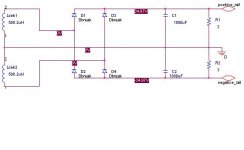
...and another idea to improve the snubbering.
If ground of the primary side and ground of the secondary are the same, then you could allow some diode paths from the switches towards the positive output rail. They can avoid high voltages across the switches and may additionally feed the energy from the leakage inductance towards the output, which should also improve efficiency.
But you need fast diodes, which can handle high currents at least for short durations.
(Please note that this snubber is only possible for designs with output voltages which are more than twice of the input voltage. Fine in your design. )
For real set up, the path through these snubbering diodes to the positive rail through the output caps back through ground, through primary supply must be short and low inductive.
Fast MKP-Caps at the output and input of the converter may help. Geometric placement should ensure the smallest possible loop.
Have fun
Markus
Attachments
 this thread....
Sorry guys i left you here with out answering for a few days... I'm in day two of whats likely to be a three day hangover...
But you are all legends! I never expected this many/quality of replies.
Heres a picture of the schematic, though you've probably seen it in the other thread already.
(Now why am I the only person who can't see it? *FDM* kicks his router).
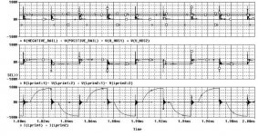
Righty - my I'm sure the FETs will be fine - the only heat sinking is the part of the PCB that the tabs were soldered to. Now just to clarify the switching process - though I think that Chocos got it right. The first FET turns on for 17.8us, then a dead time of 6us, the other turns on for 17.8us and then another dead of 6us. So 47.6us to go through the whole cycle.
IVX: no gate resistors - do there really need to be any? The BJTs that drive the gates are only signal ones.
This project was built on a shoe-string budget - the only parts I bought were the 1% resistors, the two 10% caps and the four rectification diodes. The rest of the parts were salvaged from abondoned ex-project boards at uni - including the ETD39 and a bigger core - I was quite happy to find it! I would have gone for a TL494 (I have used it in the past) but I can't get hold of one just by falling out of bed. I realised that the exact duty cycle for both halfs is very important and hence the low tolerance bits etc... I first did the calcs, then simulated, then built it. Testing it first I did it without the transformer etc, and it came out to 17.86 us for one side (gate driving voltage) and 17.90us for the other - not perfect but I think it is still close enough to prevent flux walking. Those times were the average - the scope gave different times depending what channel I plugged it into.
Schotky diodes were also on my list, but they get reasonbly expensive when they have to able to handle 90v reverse - Silicon Carbide ones would have been on my list, but I'm not that rich (yet!).
Snubbers - well I could stick em in without much trouble, and I like the idea of using them to chuck that little bit extra power through to the secondary side.
The input/output caps are definitely at the top of the improvemnt path - but I just so happened to have 200 of those 100v, 470uF electrolytics lying around - and the cost me nothing. If i can find big enough MKP caps (ohh look at that I have 33uF worth of 100V MKPs on my desk!) I'll stick them in too - but it'll required a redesigned PCB, as they shoud be closest to the rectifing diodes.
Yeah there is no air gap the core - I didn't think it would need it, but didn't do the calcs to back it up. I don't really want to rewind the transformer anytime soon. I wound it as someone had mentioned else where on this forum (primary1, secondary 1, primary 2 then secondary 2). I didn't bundle the wires up, but rather laid them out flat so it gave a very nice finish. Next time I'll probably just bundle them - it was a ***** putting on 16 wires at the same time! So if it is saturating, I can just up the frequency a bit.
Edit: It seems the auto language checker didn't like my english")
Anyway - Choco I don't have access to ORCAD but I do to Micsrosims PSpice. Will it work with that or do I have to hack up my own circuit emulation program?
But you are all legends! I never expected this many/quality of replies.
Heres a picture of the schematic, though you've probably seen it in the other thread already.
An externally hosted image should be here but it was not working when we last tested it.
(Now why am I the only person who can't see it? *FDM* kicks his router).
Righty - my I'm sure the FETs will be fine - the only heat sinking is the part of the PCB that the tabs were soldered to. Now just to clarify the switching process - though I think that Chocos got it right. The first FET turns on for 17.8us, then a dead time of 6us, the other turns on for 17.8us and then another dead of 6us. So 47.6us to go through the whole cycle.
IVX: no gate resistors - do there really need to be any? The BJTs that drive the gates are only signal ones.
Thats what I thought! I put in the BJTs and if it didn't turn it on fast enought well damn it! (it was about 6us with out the BJTs).Well, who cares. If they are cold, they are not lossy.
This project was built on a shoe-string budget - the only parts I bought were the 1% resistors, the two 10% caps and the four rectification diodes. The rest of the parts were salvaged from abondoned ex-project boards at uni - including the ETD39 and a bigger core - I was quite happy to find it! I would have gone for a TL494 (I have used it in the past) but I can't get hold of one just by falling out of bed. I realised that the exact duty cycle for both halfs is very important and hence the low tolerance bits etc... I first did the calcs, then simulated, then built it. Testing it first I did it without the transformer etc, and it came out to 17.86 us for one side (gate driving voltage) and 17.90us for the other - not perfect but I think it is still close enough to prevent flux walking. Those times were the average - the scope gave different times depending what channel I plugged it into.
Schotky diodes were also on my list, but they get reasonbly expensive when they have to able to handle 90v reverse - Silicon Carbide ones would have been on my list, but I'm not that rich (yet!).
Snubbers - well I could stick em in without much trouble, and I like the idea of using them to chuck that little bit extra power through to the secondary side.
The input/output caps are definitely at the top of the improvemnt path - but I just so happened to have 200 of those 100v, 470uF electrolytics lying around - and the cost me nothing. If i can find big enough MKP caps (ohh look at that I have 33uF worth of 100V MKPs on my desk!) I'll stick them in too - but it'll required a redesigned PCB, as they shoud be closest to the rectifing diodes.
Yeah there is no air gap the core - I didn't think it would need it, but didn't do the calcs to back it up. I don't really want to rewind the transformer anytime soon. I wound it as someone had mentioned else where on this forum (primary1, secondary 1, primary 2 then secondary 2). I didn't bundle the wires up, but rather laid them out flat so it gave a very nice finish. Next time I'll probably just bundle them - it was a ***** putting on 16 wires at the same time! So if it is saturating, I can just up the frequency a bit.
Edit: It seems the auto language checker didn't like my english
Anyway - Choco I don't have access to ORCAD but I do to Micsrosims PSpice. Will it work with that or do I have to hack up my own circuit emulation program?
ChocoHolic is right, transformer should be ok at 20khz even.
PSnce, 2 years ago, i had some problem around efficiency of the caraudio amp B52, which gives normal efficiency at up to 600w, and much less if >600w, but tl494 PWM controller was forced to unregulating state and anyway generated maximal pulse width 20us or so. Strange..
PS
nce, 2 years ago, i had some problem around efficiency of the caraudio amp B52, which gives normal efficiency at up to 600w, and much less if >600w, but tl494 PWM controller was forced to unregulating state and anyway generated maximal pulse width 20us or so. Strange..@FDM:
I think the ORCAD files will not work in the Micro Sim Design Center environment, except the netlist.....
But in fact I never went into the details for any cross usage of that files. Sorry about this.
Are you sure that there are no free evaluation versions of ORCAD in New Zealand? I am also using ORCAD Lite 9.2, which came enclosed with a book for around EUR 35 (I think)...
It has several restrictions, but I can live with that.
If I am right the Micro Sim corporation was taken over by Cadence
and they are now continuing this stuff. But there was a fundamental break between Design Center 8.xxx and ORCAD 9.xxx......
Bye
Markus
@FDM:
Great, if you want my files just send me your mail adress.
To get my simulation running, please keep the following thing in mind.
1.
The standard Ron for the switches is 1 Ohm, don't forget to adjust them.
2.
Default values in the options of the simualtion profile will not work,
because of convergence issues!
Changing the options for the simulation routine itself is sometimes critical as nearly nobody is able to foresee all the effects, which can be caused.... well, at least I am not a "GOD of Numeric Math" ....
But a very good way to get rid of 90% of all convergence issues is to allow a higher number of iterations before the simulation is aborted.
In the options of the simulation profile you will find a value which is called "ITL4". The default value here is 10 iterations, as most simualtions show very fast convergence. But especially for switching applications the SPICE algorithms often need more iterations.
If you set this value to 100, then this simulation should work.
May be my files, which I can send to you, are already including the increased ITL4 setting for this specific project...
But the Ron value of the Sbreak is given in the Sbreak.lib and you should have look to this.
Good Luck
Markus
- Status
- This old topic is closed. If you want to reopen this topic, contact a moderator using the "Report Post" button.
- Home
- Amplifiers
- Class D
- SMPS efficency issues...