This is the schematic supplied for the Amplifier Ready signal. +VB = +63V, but I think the zener diode limits the output to 5.6V. The Current limiting schematic is very similar, except it has a 4k7 series resistor before the transistor base, and the 10k resistor also becomes a 4k7 resistor.

For the clipping signal, the open collector which I have to pull up, the notes say that
the low state has a maximum of 1V.
The clipping signal may need a little special attention to make sure its transistor stays off
when input is low. Perhaps add two or three series diodes to the series base resistor.
I think the zener diode limits the output to 5.6V.
Yes, the output logic level is set to around 5V.
The clipping signal may need a little special attention to make sure its transistor stays off
when input is low. Perhaps add two or three series diodes to the series base resistor.
Is that because of the quoted 1V maximum? I wonder if it's proportional to the supplied pull-up voltage. The spec says the maximum is 65V, and given that I'll be using 15.6V I wonder if I can expect rather less than 1V.
If that's not what you're getting at, can you explain what those diodes would do?
First attempt at laying out the extra components for the LEDs:
I decided I was never going to use the speaker feedback signals - this is a 6-channel build so that I can run a pair of 3-way speakers, so each speaker cabinet will require 6 wires already; making use of the feedback signals would require 12 wires! So this gave me some extra real estate, but keeping in mind that I need to leave more space around the mounting holes I decided I still needed more space, so the board is now a bit bigger. Still has mounting holes at multiples of 10mm though, to suit the baseplate of the Dissipante chassis.
The supply voltage enters via a little Wago 2-way block, and the negative supply is grounded. I'll be using the Vdr output from my SMPS, which is intended to be used as the driver voltage for a UcD module. Apparently the UcD400OEM derives its driver voltage from the main +/-VB supply, but can save 2W if an external driver supply is provided. But if that external driver supply comes from the same supply as the +/- VB, then I guess there's no net saving. Anyway, using it the way I'm planning to, for the LEDs, will rule out using it as the external driver supply, because it would need to be referenced to -VB rather than ground.
I haven't looked at which type of transistor to use, so the footprint is the first one I found in the Eagle library, and may need to change depending on what I can buy in sensible quantities from RS, i.e. fewer than 10000 at a time!
An externally hosted image should be here but it was not working when we last tested it.
I decided I was never going to use the speaker feedback signals - this is a 6-channel build so that I can run a pair of 3-way speakers, so each speaker cabinet will require 6 wires already; making use of the feedback signals would require 12 wires! So this gave me some extra real estate, but keeping in mind that I need to leave more space around the mounting holes I decided I still needed more space, so the board is now a bit bigger. Still has mounting holes at multiples of 10mm though, to suit the baseplate of the Dissipante chassis.
The supply voltage enters via a little Wago 2-way block, and the negative supply is grounded. I'll be using the Vdr output from my SMPS, which is intended to be used as the driver voltage for a UcD module. Apparently the UcD400OEM derives its driver voltage from the main +/-VB supply, but can save 2W if an external driver supply is provided. But if that external driver supply comes from the same supply as the +/- VB, then I guess there's no net saving. Anyway, using it the way I'm planning to, for the LEDs, will rule out using it as the external driver supply, because it would need to be referenced to -VB rather than ground.
I haven't looked at which type of transistor to use, so the footprint is the first one I found in the Eagle library, and may need to change depending on what I can buy in sensible quantities from RS, i.e. fewer than 10000 at a time!
My UCD full discrete construction.😀😀😀😀
Can you elaborate? What are we seeing in the photo? Is that a power supply that you've built yourself?
I've had a go at designing the other two circuits for the front panel lights.
Recap:
- Amp(s) Ready: This light needs to be ON when ALL of the amps are ready, i.e. when all 6 Amp Ready pins are LOW. Rayma's advice that this is a NOR circuit, and his sample schematic helped a lot here.
Now the 'Clipping' and 'Current Limiting' circuits. These need different circuits.
- Current Limiting: This light needs to be OFF when NONE of the amps is limiting, but come on when ANY of the amps is limiting, i.e. when any of the 6 Current Limiting pins is LOW. So I think this makes it a NAND circuit. So this means I need a separate pull-up resistor for the transistor base (so it's high by default), and the diodes need to be the other way round, so that the transistor base goes low if any of the input pins goes low.
- Clipping: This works the same way as the Current Limiting circuit. The difference is that these pins are open collectors (not internally pulled up), but since my individual adapter boards will pull them up I think this makes the required circuit identical to the Current Limiting circuit.
So here is my schematic for these circuits. The idea is that the three pins from each amplifier adapter board will be brought onto the board via the 6x 3-pin headers JP1 to JP6, and the supply for the board will be the same 15.6V as used by the adapter boards. The three LEDs can either be fixed to the board or connected via flyleads.

And here's what the PCB could look like:

Recap:
- Amp(s) Ready: This light needs to be ON when ALL of the amps are ready, i.e. when all 6 Amp Ready pins are LOW. Rayma's advice that this is a NOR circuit, and his sample schematic helped a lot here.
Now the 'Clipping' and 'Current Limiting' circuits. These need different circuits.
- Current Limiting: This light needs to be OFF when NONE of the amps is limiting, but come on when ANY of the amps is limiting, i.e. when any of the 6 Current Limiting pins is LOW. So I think this makes it a NAND circuit. So this means I need a separate pull-up resistor for the transistor base (so it's high by default), and the diodes need to be the other way round, so that the transistor base goes low if any of the input pins goes low.
- Clipping: This works the same way as the Current Limiting circuit. The difference is that these pins are open collectors (not internally pulled up), but since my individual adapter boards will pull them up I think this makes the required circuit identical to the Current Limiting circuit.
So here is my schematic for these circuits. The idea is that the three pins from each amplifier adapter board will be brought onto the board via the 6x 3-pin headers JP1 to JP6, and the supply for the board will be the same 15.6V as used by the adapter boards. The three LEDs can either be fixed to the board or connected via flyleads.
And here's what the PCB could look like:
In case it isn't obvious, I'm really not sure whether I'm doing this correctly, so please feel free to point out the obvious blunders! Also, Rayma's earlier comment, about the clipping signal needing special attention, needs to be addressed, but I didn't understand the problem or the proposed solution.
In the meantime, I went back to the CAD drawing to make sure there's room for the bigger adapter boards and the LED control panel. It all still fits - just. I may aim to mount the LED PCB vertically on the inside of the front panel, so that the LEDs align directly with the corresponding holes in the front panel. It would save space on the baseplate, and avoid having to run flyleads between the front panel and the PCB.
In the meantime, I went back to the CAD drawing to make sure there's room for the bigger adapter boards and the LED control panel. It all still fits - just. I may aim to mount the LED PCB vertically on the inside of the front panel, so that the LEDs align directly with the corresponding holes in the front panel. It would save space on the baseplate, and avoid having to run flyleads between the front panel and the PCB.
An externally hosted image should be here but it was not working when we last tested it.
I made a replacement ribbon cable between the DLCP and the input panel, so that I could break out the USB lines to pass them through the little dedicated relay board that I made. This is to allow me to have the internal Raspberry Pi as the default USB source, and also leave the option to connect another USB source, or especially a PC to control the DLCP, to the external USB input - the power from the external device switches the relays over to disconnect the RPi.
And here's the Raspberry Pi that I'm going to mount to the inside of the front panel, complete with my button panel which precisely mirrors the DLCP control panel buttons. The RPi is running LMS and Squeezelite (through piCorePlayer), so it'll act as my Squeezebox server and my default player.
The little PCB on the bottom of the stack is a mains-to-5VDC 2.3A power supply, which is apparently the same one used in the Squeezebox Transporter. Conveniently two of the mounting holes in the power supply are at exactly the same spacing as the RPi mounting holes. The plastic stilts are just there so the stack stands flat while I'm experimenting with it on the bench.
An externally hosted image should be here but it was not working when we last tested it.
Since this is a 6-channel integrated amplifier, I wanted the option to use the DSP and power amp stages separately. I haven't got room on the back panel to add 6 balanced XLR sockets for the DLCP outputs AND 6 balanced XLR sockets for the UcD inputs, so I made a little board with the same Molex sockets as the DLCP. I also used the same socket for the input on the UcD adapter board. This is it with some sockets placed loosely along one edge of each board. The white mounting blocks are bespoke items I made with a 3D printer.
I originally planned to make little balanced jumpers to link the outputs to the inputs, but I think I'll probably just bypass these boards altogether initially, and if I need to use the stages separately in the future then I can just take the lid of and move some cables around.
An externally hosted image should be here but it was not working when we last tested it.
.I originally planned to make little balanced jumpers to link the outputs to the inputs, but I think I'll probably just bypass these boards altogether initially, and if I need to use the stages separately in the future then I can just take the lid of and move some cables around.
Current Limiting: This light needs to be OFF when NONE of the amps is limiting, but come on when ANY of the amps is limiting, i.e. when any of the 6 Current Limiting pins is LOW. So I think this makes it a NAND circuit. So this means I need a separate pull-up resistor for the transistor base (so it's high by default), and the diodes need to be the other way round, so that the transistor base goes low if any of the input pins goes low.
- Clipping: This works the same way as the Current Limiting circuit.
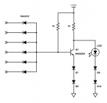
Here's a six input nand gate. It may be possible to combine the 4 diodes into just two,
shared between the LED and the transistor.
Attachments
Current Limiting: This light needs to be OFF when NONE of the amps is limiting, but come on when ANY of the amps is limiting, i.e. when any of the 6 Current Limiting pins is LOW. So I think this makes it a NAND circuit. So this means I need a separate pull-up resistor for the transistor base (so it's high by default), and the diodes need to be the other way round, so that the transistor base goes low if any of the input pins goes low.
- Clipping: This works the same way as the Current Limiting circuit.
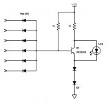
Here's a reduced version of the NAND gate.
Attachments
Thank you - I'll add a couple of diodes to the NAND circuits. From our PMs I gather these diodes will raise the voltage on the emitter of the transistor, so that the base is guaranteed to be low enough (compared to the emitter) to turn off the transistor. So those two diodes will cope even when the clipping circuit is at it's worst case of 1V.
Your help is much appreciated.
Your help is much appreciated.
The updated schematic, with the added diodes:
And a draft of the corresponding PCB:
An externally hosted image should be here but it was not working when we last tested it.
And a draft of the corresponding PCB:
An externally hosted image should be here but it was not working when we last tested it.
The updated schematic, with the added diodes
If logic "off" is 0VDC, you should not need the input resistors for the NAND,
just the diode anodes connected to the base. Those resistors are needed for the NOR.
Also for the NOR only, I would also add a 10k resistor from the base to ground.
Last edited:
Ooh, that's good - should save quite a lot of soldering!
(I take it you mean R7 to R18?)
Yes, that's right.
Last edited:
Here's the schematic with those input resistors removed (I forgot to renumber R19 to R23, but I'll do that before placing an order):
And here's the simplified PCB. I tired to lay it out so that the diode directions correspond to their direction in the schematic - components can go anywhere in any orientation on the PCB itself, as long as the traces between them are correct, but I wanted the logic to be somewhat self-explanatory.
Just need to figure which LEDs to use for the front panel (and how to fix them in place), then what resistor values to use. The DLCP also has a 'Power On' LED header, so I'm envisaging 4 front panel LEDs in a row - 'Power', 'Amps Ready', 'Current Limiting' and 'Clipping'.
An externally hosted image should be here but it was not working when we last tested it.
And here's the simplified PCB. I tired to lay it out so that the diode directions correspond to their direction in the schematic - components can go anywhere in any orientation on the PCB itself, as long as the traces between them are correct, but I wanted the logic to be somewhat self-explanatory.
An externally hosted image should be here but it was not working when we last tested it.
Just need to figure which LEDs to use for the front panel (and how to fix them in place), then what resistor values to use. The DLCP also has a 'Power On' LED header, so I'm envisaging 4 front panel LEDs in a row - 'Power', 'Amps Ready', 'Current Limiting' and 'Clipping'.
There are lots of snap-in types.Just need to figure which LEDs to use for the front panel (and how to fix them in place).
SSI-LXH312GD-150 Lumex Opto/Components Inc. | Optoelectronics | DigiKey
- Status
- This old topic is closed. If you want to reopen this topic, contact a moderator using the "Report Post" button.
- Home
- Amplifiers
- Class D
- Hypex DLCP/UcD400 build