ok so to spur some advice/discussion, im doing some pretty pictures!
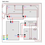
attached here is the basic wiring layout inside the amp, before grounding/shelding is considered.
ive simplified it somewhat (only one channel per amp is shown, and im ignoring the other inputs/outputs of the minidsp)
assume all signal and power would be twisted pairs.
attached here is the basic wiring layout inside the amp, before grounding/shelding is considered.
ive simplified it somewhat (only one channel per amp is shown, and im ignoring the other inputs/outputs of the minidsp)
assume all signal and power would be twisted pairs.
Attachments
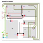
now here is my proposed shielding/grounding setup.
signal cables are two core with a shield.
as per this guide:
Grounding and Shielding for your DIY Audio Projects
im using the input rca jack as a common grounding point. rca jacks are isolated from case.
all signal grounds are connected together at one end (of stereo pair) and shield is connected to the same point, again, only at one end.
i might possibly need some kind of isolation for the chassis ground ( ive seen people mentioning capacitor/resistor, bridge rectifier etc) but i still need to get my head round that.
anyone care to point out any grave errors? this subject seems a minefield.
EDIT: just noticed i connected the shields and grounds on the rear rca inputs together at both ends. an artworking error. they would not be connected at the minidsp end for those cables.
Attachments
Last edited:
one element i forgot to include in drawing, is that the 3255 chips on the amp board are earthed to the chassis through the heatsink.
no idea if this is a problem.
also note, there is an aluminium partition/wall around the smps, which is, obviously electrically part of the chassis.
no idea if this is a problem.
also note, there is an aluminium partition/wall around the smps, which is, obviously electrically part of the chassis.
Last edited:
possibly i am confused between pwr gnd on the 48v side, and the mains gnd (earth) connection.
in that guide, paragraph 6 states:
" At the input jack ground I connect a single wire from the power supply ground." i assumed that referred to the earth connection on the mains side of the psu.
in that guide, paragraph 6 states:
" At the input jack ground I connect a single wire from the power supply ground." i assumed that referred to the earth connection on the mains side of the psu.
Not sure if you were going to use SE inputs, but if so I found this interesting...
http://www.ti.com/lit/an/slaa719/slaa719.pdf
I couldn't if/how to do this to the EVM.
Mike
http://www.ti.com/lit/an/slaa719/slaa719.pdf
I couldn't if/how to do this to the EVM.
Mike
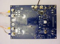
Not sure what, if anything, can be done. I think R38, C70, and C72 are the VMid components, but can't tell if they connect to the ground plane or have separate traces. Also not sure if the GND via on the bottom of the board is the board star ground.
Sorry if I muddied up the conversation.
Sorry if I muddied up the conversation.
well handily the psu has two isolated aux supplies, so maybe ill run the minidsp from one, and the bt module from the other.
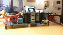
i am concerned about the 3255 chips being basically connected to the chassis through the heatsink.
Should i place a silicone heatpad between the heatsink and the heatpipe block (connected to chip via heatpipe and another block) ? at that point its a large surface area so shouldnt impede heatflow too much.
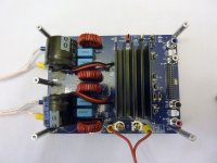
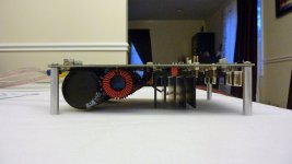
ha.. thanks for the suggestion.. i avoided that since i read that the big capacitors have to be as close to the amp as possible.. anyway, im still neck deep in my project, but i received my heatsinking components today, so this is the first time ive mounted the amps together.
the block there is connected to the heatsink with 4x 45watt heatpipes.
i dont think you can get much more "spacesaver" with these boards.
the block there is connected to the heatsink with 4x 45watt heatpipes.
i dont think you can get much more "spacesaver" with these boards.
Attachments
ha.. thanks for the suggestion.. i avoided that since i read that the big capacitors have to be as close to the amp as possible..
True story for holding THD down.
- Status
- This old topic is closed. If you want to reopen this topic, contact a moderator using the "Report Post" button.
- Home
- Amplifiers
- Class D
- tpa3255evm spacesaver mod