yes.. yes i could..
that would of course require a much more precise 3d model than i have created, modelling the heatsink including the fine ribbing.( its been created to check if things fit in the box, work out shielding, and do wire routing, no more)
It would also require learning fusion 360, and rather more about FEM analysis than i already know ( i use it for softbody dynamic simulations sometimes for work..)
Sometimes "its way, way bigger than the stock heatsink, and the thermal interfaces are 16x larger than the chip heatpad" should be enough to eyeball it .. no?
id imagine somebody with experience such as yourself could look at my description, and the heatsink in the link, and know in one second if it would likely be sufficient or not... for me, it looks fine... but ive not got so much experience.
Robin--can you throw out a screenshot of the wireframe (or a quick render?). I'm not following your layout that well. Essentially you're bolting 2 such boards to a 2x4 cm bar stock, which then is end-bolted to the heatsink? To a first order, that seems to be grossly underutilizing your heat sink area on said box. Is there something preventing you from making a larger, if less pretty bolt-on aluminum spacer that would allow you to place the two boards horizontally down the length of the heatsink (and thus actually take full advantage of said heatsink)? Some careful work with sandpaper (up to maybe 1000 grit?) will give you more than enough polish to keep the heatsink paste thin.
yeah sure.. ill knock a quick screengrab out.
from my perspective the main design limitation is the fact of 2 thermal junctions between chip and heatsink.. not very efficient. obviously the size of the first junction is limited by the heatpad on the chip .. the second, by the crossection of the stock i choose, which could be bigger if necessary.
mounting the evm directly to a large heatsink is pretty impossible given the board layout, and even directly mounted, youd only have like 1cm2 of contact with heatsink (the size of 2 of the heatpads)
screngrab to follow
Even if x1000, you won't get away more heat due to limited heat conducting area.Sometimes "its way, way bigger than the stock heatsink, and the thermal interfaces are 16x larger than the chip heatpad" should be enough to eyeball it .. no?
Some background info for thermal transfer on TPA3251:
Silicon thickness: 0.4mm
Silicon conductivity: 0.117 W/mmK
heat conducting area: ~15mm^2 (assuming mostly from powerFETs)
Silicon: Theta J-DA= 0.23 degC/W
Die attach thickness: 0.05mm
Die Attach conductivity: 0.006 W/mmK
Die attach area ~25 mm^2
Die attach to Case: Theta DA-Case= 0.33 degC/W
Total Theta JC = 0.23+0.33= 0.56 degC/W
Copper heat pad thermal resistance should be negligible, but it needs to help spread the heat from the internal die attach area to a total external pad area of 48mm^2 (12mm x 4mm). Use an effective area somewhere between 25 and 48mm^2 to calculate the heat sink grease thermal resistance.
As a bench experiment, to calibrate thermal assumptions use the OTW warning to help read the internal die temperature of 125C at different power dissipation levels/heat sink combinations. You also need to know (total power in) - (total power out) to know the dissipation.
I use up to 1500. It is important to have very good coplanarity between heatslug and mounting surface + heatsink mounting to the board.Some careful work with sandpaper (up to maybe 1000 grit?)
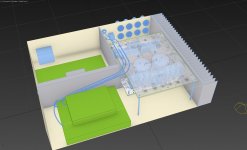
here is a quick screengrab of my current layout proposal. obviously incomplete..
the top evm is shown ghosted so you can see the alu bar below, and the bottom evm below that.
two green boxes in foreground are minidsp and bluetooth receiver.
green plane in seperate (shielded) compartment at back is PSU.
you can just see an aluminium block on top of psu which replacces heatsink there. this is bolted to 1cm thick plate in front of it, which is in turn bolted/thermal greased to bottom and other side of case. i figured that would be sufficient to transfer psu heat to case exterior..
Attachments
Even if x1000, you won't get away more heat due to limited heat conducting area.
this sounds like you are suggesting that a larger heatsink wont keep the chip cooler.. ? in that case neither would forced air..?
im not 100% sure i follow.. why am i basically not using the heatsink.?
assuming i can get good thermal contact between the end of the bar, and the heatsink, it would be conceptually similar (although not as performant) as a single piece of aluminium with the chips attached on one end, and the heatsink fins on the other. (a big "T" shaped heatsink )
considering the contact area between the bar and the heatsink is 8cm2 (could be bigger of course, i could double it without changing the design too much)
and the contact area of both chips (combined) is less than 1cm2 id imagine the bar/heatsink junction thermal resistance would be much much smaller than the chip/bar junction..
rotating the boards 90 degrees would require a different case and design.. possible of course if necessary.
in the end its the same concept as "heatpipe" designs, just with a massive aluminium block in place of a heatpipe..
see here:
http://zelfbouwaudio.nl/forum/download/file.php?id=109472&mode=view
Last edited:
this sounds like you are suggesting that a larger heatsink wont keep the chip cooler.. ? in that case neither would forced air..?
My intentional saying is that the conducting area is not limited by the heatsink but the outputstage-FET-area of the TPA32XX IC. (Which is rougly ~15mm^2)
(A not unusual non-native-speaker understandingly problem
 - what a sentence..)
Because you're contacting a single 8 cm^2 section in the middle of the heat sink and assuming it will spread the heat out past the couple nearest fins, which is really doubtful. You'll have a massive heat gradient from the center of the heat sink to the fins at the front/back extremities.
Having two point sources and a horizontal heat spreader bar at least helps you get more out of the heat sink you have.
Edit--also what the good doctor wrote, although having a large aluminum block is going to help "absorb" transient heat better than the EVM heatsink.
Having two point sources and a horizontal heat spreader bar at least helps you get more out of the heat sink you have.
Edit--also what the good doctor wrote, although having a large aluminum block is going to help "absorb" transient heat better than the EVM heatsink.
Last edited:
My intentional saying is that the conducting area is not limited by the heatsink but the outputstage-FET-area of the TPA32XX IC. (Which is rougly ~15mm^2)
(A not unusual non-native-speaker understandingly problem
yes i understand that.. which is why i assumed that a thermal contact of 8cm square between aluminium bar and case heatsink would not be a limiting factor.. its already many times more conductive than the chip junction..
in any case, im going to look at increasing the spacing of the chips along the heatsink , see if i can get them to warm up different bits of the 'sink..
thanks for the input guys!
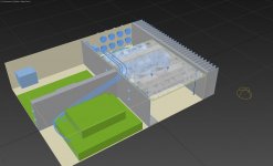
ok.. new version with top amp flipped round, and moved as far to back of case as possible.
this allows 2x slimmer aluminium bars. one 4cm x 1.2cm cross section bar for each amp.
heat should be spread more evenly across heatsink in this case.
in the end, even if i managed to find a magic way to mount both chips directly to heatsink, they would be very "hotspotty" due to the tiny chips!
this allows 2x slimmer aluminium bars. one 4cm x 1.2cm cross section bar for each amp.
heat should be spread more evenly across heatsink in this case.
in the end, even if i managed to find a magic way to mount both chips directly to heatsink, they would be very "hotspotty" due to the tiny chips!
Attachments
Better!
Instead of skinny and tall, can you fit as large a square bar in between the large capacitors and other circuitry? E.g. 2 cm x 2 cm. Essentially trying to get as much horizontal coverage as possible. The giant slug of aluminum known as the bar will definitely help with thermal transients.
Instead of skinny and tall, can you fit as large a square bar in between the large capacitors and other circuitry? E.g. 2 cm x 2 cm. Essentially trying to get as much horizontal coverage as possible. The giant slug of aluminum known as the bar will definitely help with thermal transients.
with the amps this way round, thats about the limit in the space ive got.. particularly the front amp, there is only 15 mm horizontally between the big caps on that, and the inductors on the back amp.. so i think thats about as far as i can go.
i need to wait till the amps arrive before knowing exactly how much space i have in reality.. could be a few mm out here and there!
i need to wait till the amps arrive before knowing exactly how much space i have in reality.. could be a few mm out here and there!
unless i am mistaken, its a bad idea to use copper and aluminium together in this way.. you get galvanic reactions.. heatsink is alu, so i should keep it all-alu..?
plus copper bar is rather costy!
edit: i was getting mixed up with watercooling setups, of which i have built many. there you get galvanic corrosion if you use aluminium and copper in the same water loop..
so, i guess this is doable.. but would it be worth the large extra expense?
plus copper bar is rather costy!
edit: i was getting mixed up with watercooling setups, of which i have built many. there you get galvanic corrosion if you use aluminium and copper in the same water loop..
so, i guess this is doable.. but would it be worth the large extra expense?
Last edited:
Ok a quick update and a change of subject.
Re. Cooling, ive modified the design to use heatpipes, 2x 45w rated 6mm ones for each board. Contact along almost full length of heatsink. I had hoped to use a copper block on the chip side, but i require a machined block 2cmx5x5, and i was quoted 50 euros for it, so im going with aluminium. Hope that a) i can get a tight enough fitting hole drilled for the pipes that i can still slide them into. Guess thermal paste will help on both counts. B) that i can bend then without breaking any! Ive ordered the number i need, as they are not cheap.
Now onto grounding. Something written a lot about i know.
However i have a couple of basic questions before starting.
Im planning to star earth where possible. I assume that the pcbs should be on insulating mounts in this case, with a single earth going to the star point. However, the chips will be earthed to the case via heatsink. Should i put an insulating sheet between heatpipe block and heatsink, or keep that grounding path?
I was also planning to keep signal ground seperate, and use conductive sleeving over all twisted signal and mains cabling, (earthed to star point?) sound ok? Worth doing?
Finally, i have a minidsp and Bluetooth reciever running from 12v from main psu. I was going to isolate these from the chassis too.
Cheers!
Ps. Now i have all the bits, fitting the amps in will be a challenge! I ignored some components and case intrusions in my 3d layout. will need to remove rca jacks from amps and possibly bend some jumpers over 90 degrees. Sheesh.
- Status
- This old topic is closed. If you want to reopen this topic, contact a moderator using the "Report Post" button.
- Home
- Amplifiers
- Class D
- tpa3255evm spacesaver mod