Hello all,
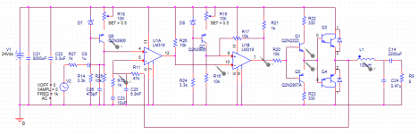
I have recently been working on a self-oscillating class D design that uses hysteresis and feedback based around the LM319 dual comparator. The first comparator is used as an error comparator of the input and feedback loop, while the second comparator is used as a Schmitt trigger inverter to generate the PWM signal to drive the power stage. The Darlington power transistors I am using for Q3 and Q4 are TIP102 and TIP107 respectively, and the zener diodes D7 and D8 used in the biasing sections are actually each two blue LEDs in series.
So far, initial signs are that the design works reasonably well, but I am having some issues with the power transistors getting hotter than they should be. I believe that this is due to voltage spikes caused by the heavily inductive load that are then being dissipated through the back diodes of the power transistors.
If I am correct in my reasoning for this problem, what would be the best way to mitigate the reactive loading at the output? Additionally, does anyone have any corrections or suggestions for improvements to this design? I make no claims that this design is even remotely good or even a safe design, so please don't assume that anything on here is correct.
Truth be told, I have designed this almost entirely without the aid of simulation as all my attempts so far seem to throw convergence errors (the attached PSpice schematic is not an actual simulation). I eventually plan to modify this design for higher power and a full bridge at a later date, but as it stands, this design is just an experiment, and I can't move forward until I figure out what is causing this design to overheat.
(p.s. it seems from looking around that most here are using integrated class D chips for their designs rather than more discrete components. Is there any possibility that this thread would be better suited to the solid state subforum for this reason?)
I have recently been working on a self-oscillating class D design that uses hysteresis and feedback based around the LM319 dual comparator. The first comparator is used as an error comparator of the input and feedback loop, while the second comparator is used as a Schmitt trigger inverter to generate the PWM signal to drive the power stage. The Darlington power transistors I am using for Q3 and Q4 are TIP102 and TIP107 respectively, and the zener diodes D7 and D8 used in the biasing sections are actually each two blue LEDs in series.
So far, initial signs are that the design works reasonably well, but I am having some issues with the power transistors getting hotter than they should be. I believe that this is due to voltage spikes caused by the heavily inductive load that are then being dissipated through the back diodes of the power transistors.
If I am correct in my reasoning for this problem, what would be the best way to mitigate the reactive loading at the output? Additionally, does anyone have any corrections or suggestions for improvements to this design? I make no claims that this design is even remotely good or even a safe design, so please don't assume that anything on here is correct.
Truth be told, I have designed this almost entirely without the aid of simulation as all my attempts so far seem to throw convergence errors
(the attached PSpice schematic is not an actual simulation). I eventually plan to modify this design for higher power and a full bridge at a later date, but as it stands, this design is just an experiment, and I can't move forward until I figure out what is causing this design to overheat.(p.s. it seems from looking around that most here are using integrated class D chips for their designs rather than more discrete components. Is there any possibility that this thread would be better suited to the solid state subforum for this reason?)
Attachments
I am having some issues with the power transistors getting hotter than they should be.
I believe that this is due to voltage spikes caused by the heavily inductive load that are then
being dissipated through the back diodes of the power transistors.
Try Schottky power diodes in anti-parallel with the outputs. They should absorb some of the currents
without the body diodes turning on, if connected with a low inductance path.
Last edited:
Try Schottky power diodes in anti-parallel with the outputs. They should absorb some of the currents
without the body diodes turning on, if connected with a low inductance path.
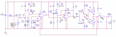
Ok, cool. I dug through my junk box and found some SR360 Schottky diodes which I tacked on. I assume by anti-parallel you just mean across the body diodes in exactly the same way? Either way, I tested it just now, and this seems to have significantly reduced the heat at the power transistors. See the updated schematic with the addition of D9 and D10. Thanks for the quick response, by the way!
Any other suggestions from anybody? This is my first time designing a class D amp, so I imagine there are other improvements to be made here. I'm open to anything, really. I'm mainly doing this as a learning exercise.
Attachments
This is my first time designing a class D amp, so I imagine there are other improvements to be made here.
Why Darlingtons? Also, you'll likely need a ground plane pcb for this circuit.
The pulldown resistor R26 value of 10k may be too large for fast switching.
Maybe better drivers, like 2N4401/2N4403 instead of 2N2222/2N2907.
Last edited:
Why Darlingtons?
Maybe a better driver, like 2N4401/2N4403 instead of 2N2222/2N2907.
Darlingtons because I had originally tried to design this without the Q1/Q5 driver stage, and the input capacitance of FETs would be too high. That isn't really an issue anymore, so FETs would definitely work here. It didn't really work without the driver, although maybe it would work better now that the body diode issue is fixed. That said, the Darlingtons seem to work reasonably well here, so would there be much benefit to switching over to FETs?
As for the driver, well, it's funny you should mention that. They actually ARE a 2N4401/2N4403 pair, just Pspice doesn't have those in their library. I suppose I should have mentioned that, but I didn't think it would matter enough for anyone to mention it.
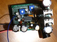
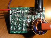
What would be the advantage of the ground plane? protection from high frequency noise, I assume? I tried to keep the layout as tight as possible, but I agree that a proper PCB with a ground plane would be better.
Last edited:
Darlingtons because I had originally tried to design this without the Q1/Q5 driver stage,
and the input capacitance of FETs would be too high. That isn't really an issue anymore.
It didn't really work without the driver, although maybe it would work better now that
the body diode issue is fixed.
I'd go back to the FETs with this driver stage, but remember that the gate/source drive voltage is 15V.
Also, maybe move the two 330R to the drivers' emitters, instead of at the collectors.
It's a lot more difficult to make a good breadboard, then a good pcb with a ground plane.
Last edited:
Okay, so I tried reducing the pull-up resistor R26 to about 2.5K by putting a 3.3k resistor in parallel with the existing one. No real effect. If anything it reduced the switching frequency from about 700KHz to approximately 600KHz at idle. The LM319 is pretty fast at the inputs, but may not have a lot of drive capability at the outputs, so I imagine that at some point the pull-down current becomes more of a limiting factor than the input capacitance. Actually, I suspect that the switching speed of U1B is the bottleneck on this system. What would you consider to be a "good" switching frequency for something like this?
One thing I did try was shorting the 330-Ohm resistors R22 and R23, and although it didn't significantly effect the switching frequency, this seems to have improved the rise time and reduced the heat produced by the power stage. Unfortunately, it seems to have also increased noise at the output somewhat, so I may have to compromise and lower the value of R22/R23 without shorting them entirely.
I might try replacing the power stage with FETs, but the issue of the gate-source breakdown voltage is a conern for me. I also don't have very good parts on hand for a FET pair, so I may have to save that for a later date.
Last edited:
I imagine that at some point the pull-down current becomes more of a limiting factor than the input capacitance.
At such a high switching frequency, you'll need the whole bag of tricks. The faster the transition time,
the lower the switching loss, so run all the pulldowns at the minimum resistance. Use a ground plane,
with all smt packages for the control circuit.
Last edited:
Ok, cool. I dug through my junk box and found some SR360 Schottky diodes which I tacked on. I assume by anti-parallel you just mean across the body diodes in exactly the same way? Either way, I tested it just now, and this seems to have significantly reduced the heat at the power transistors. See the updated schematic with the addition of D9 and D10. Thanks for the quick response, by the way!
Any other suggestions from anybody? This is my first time designing a class D amp, so I imagine there are other improvements to be made here. I'm open to anything, really. I'm mainly doing this as a learning exercise.
Good first attempt, but many things can be optimised.
Feedback concept: since your second comparator is driven by square wave, it cannot really considered as histeretic feedback. It uniforms and delays the PWM signal transitions. The basic topology is delay controlled, which is not the best... phase controlled and histeretic controls are both better. You can add histeresis to first stage, or other poles to the feedback loop. Changing first comparator to integrator (plus phase shifter) is also good. 600 kHz sw freq is not neccessary for good control, and too high for efficient operation.
Power stage: you can definitely reach much lower conduction loss with MOSFETs (0.1-0.3 V vs. 2.5 V drop), and significantly lower switching loss, however its hard to compare, since darlingtons are not specified for this at the mode you use it. Using MOSFETs is not trivial if you came from the world of bipolar devices, but there are a couple of good methods. You can even find multiple chanell of complete power stages in ICs if you don't want to mess with the details.
Filter: inductance is too high. At 20 kHz you will get too much drop. UCD style feedback topology (phase-shift based, post-filter, self oscillating) can make output stable, but fast large signal response still requires lower inductance.
- Status
- This old topic is closed. If you want to reopen this topic, contact a moderator using the "Report Post" button.
- Home
- Amplifiers
- Class D
- self-oscillating hysteresis-based class D using LM319, seeking advice/critique