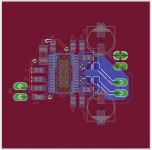
Looks nice for a first approach. You could achieve a better heat flow by connecting the top thermal pad widely to the top gnd layer.")
Personally I do not like the idea of "inductorless" class-D-amps very much but prefer LC output filter to reduce output pwm ripple.
Personally I do not like the idea of "inductorless" class-D-amps very much but prefer LC output filter to reduce output pwm ripple.
Last edited:
Thank you voltwide. I appreciate the input!
I meant to ask in my first post how I would acheive getting the gnd plane better connected at each end of the chip. I could NOT figure that out lol. For a long time I couldn't even get the thermal pad connected to gnd at all then I finally managed that but when I fill a polygon it just gives me those small connections.
"Personally I do not like the idea of "inductorless" class-D-amps very much but prefer LC output filter to reduce output pwm ripple."
I've read much about this and decided to just keep it simple(and cheap) for my first run. The output leads will not be longer than a few inches give or take. I'll consider changing it though because I certainly have the space.
Thanks again!
- Status
- This old topic is closed. If you want to reopen this topic, contact a moderator using the "Report Post" button.