Hi,there
i have always been fascinated with Class- D amplifiers, because of their efficiency and elegance. So I started small and made a 200W @ 4E amp using IRS2092 and IRFB4227PBF ,it works fine and is nearly indestructible,it has a flat response from 20hz to 20Khz with a slight peaking above 35khz ,it includes DC- protection ,clip pop removal , thermal + shortcircuit protection,signal presence and clip indicator with a option of interface with a VCA .
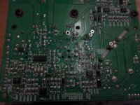
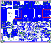
So coming to the point ,i would like to scale up the power of my current module.I have been following the iraudamp9 application note from IR and been following threads here and there and come to the conclusion that PCB layout is paramount ,so i would like to share the PCB design of my current 1200W@2E for pointers if iam doing it right or wrong .
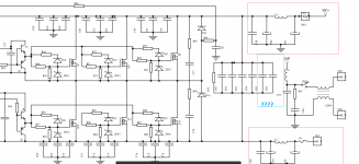
Attached pics and schematic of the current 200W @4E , I will not be including values of the components or the complete PCB layout as i dont want the design to copied endlessly as everyone knows how time consuming and painstaking it is to design a reliable Class-D amp.i would definitely share my entire work with people who are true to the diy spirit and give valid pointers on my work ...
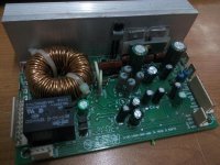
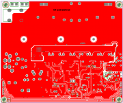
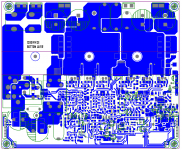
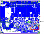
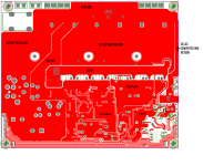
Also attaching some uncompleted PCB top and bottom layer for the 1200W@2E screen shots , Iwill be coming up with the schematic shortly ,its all in parts and pieces on the drawing board....
Cheers All
i have always been fascinated with Class- D amplifiers, because of their efficiency and elegance. So I started small and made a 200W @ 4E amp using IRS2092 and IRFB4227PBF ,it works fine and is nearly indestructible,it has a flat response from 20hz to 20Khz with a slight peaking above 35khz ,it includes DC- protection ,clip pop removal , thermal + shortcircuit protection,signal presence and clip indicator with a option of interface with a VCA .
So coming to the point ,i would like to scale up the power of my current module.I have been following the iraudamp9 application note from IR and been following threads here and there and come to the conclusion that PCB layout is paramount ,so i would like to share the PCB design of my current 1200W@2E for pointers if iam doing it right or wrong .
Attached pics and schematic of the current 200W @4E , I will not be including values of the components or the complete PCB layout as i dont want the design to copied endlessly as everyone knows how time consuming and painstaking it is to design a reliable Class-D amp.i would definitely share my entire work with people who are true to the diy spirit and give valid pointers on my work ...
Also attaching some uncompleted PCB top and bottom layer for the 1200W@2E screen shots , Iwill be coming up with the schematic shortly ,its all in parts and pieces on the drawing board....
Cheers All
Attachments
")
the additional diode and resistor is used for select able fall time for the mosfets .. and the snubber is there see in the marked red box ... and the bottom layer are basically +Vcc & -Vcc only top layer is ground ... and thanks for the pointing out the layout issues ....
Attachments
Glad to see a design contribution again.
A first view to your PCB looks like you have spend some thoughts on keeping low the inductances of the most crucial loops - keeping fingers crossed.
Components:
- The picture of your older version shows the output filter choke with dual or
triple layer winding. Single layer is definitely preferable in terms of parasitic winding capacitance.
- You should have a look to the AC current stress of C90 and C92.
It is hard to judge without knowing your switching frequency + rail voltages + inductance of the output choke ... but seeing the target power and load impedance, it is likely that already the current ripple during idle is critical for average e-caps.
I agree, PCB looks great, nothing too wrong with it, I also agree about caps. I would expect more caps per rail to share the current, using only one at high power levels will overheat it.
Is that the best way to get Vcc for IRS at those higher voltages? I can't remember, what was the current draw (dependent on switching freq of course), but I know a lot of heat was generated. Sure, it is one of the easiest ways that way, but you might want to thing about some other option
Is that the best way to get Vcc for IRS at those higher voltages? I can't remember, what was the current draw (dependent on switching freq of course), but I know a lot of heat was generated. Sure, it is one of the easiest ways that way, but you might want to thing about some other option
Last edited:
dear luka and chocoholic , thanks for the reply the mentioned caps are at least 1000uf/100V low ESR variant electrolytic and including the inductors they form a LC pass filter do that the high frequency switching ripple do not pass through (see marked in red),i read some were that big through hole metalized polyester capacitors across the high side mosfet drain and low side source are not effective, instead X7R type SMD capacitors are better , kindly confirm my thoughts(see marked in blue with qustion mark)
Regards
Regards
Attachments
The X7R types are good to catch HF ringing in the 10MHz...300MHz range and
it is crucial to have them closest possible at the MosFets.
However the fundamental and some higher orders of the current ripple which results from switching pos and neg voltages to the inductor of the of the output filter will be shared according the capacitance values of the rail caps.
You will find it almost completely in C90 and C92. The e-caps on the other side of the supply rail choke will get much less ripple current (as desired in terms keeping ripple away from the external wirings).
Low ESR is necessary, yes. However this does not mean than any current is allowed. Have a look to the ripple current specification of the cap and check if your ripple load in C90 and C92 is really below that - should even offer some headroom.
Hint:
Pick LT spice and simulate a simplified half bridge with output filter in idle situation.
You will get a triangular current in the choke of the output filter.
This triangular current is conducted in alternating manner from the high side MosFet or the low side MosFet. The MosFet currents will be seen in the corresponding rail cap.
can i use the following app note equations to calculate the required ceramic capacitors .
http://www.ti.com/lit/an/slta055/slta055.pdf
regards
http://www.ti.com/lit/an/slta055/slta055.pdf
regards
so after reading and checking out couple of discussion on the forum , i decided it is best to use X7R smd capacitors for decoupling purpose so no more MPP or MKP on the DC BUS ..As of now the bypass capacitors are being changed to SMD ... Do correct me if i am wrong ..
Regards
Regards
Please take care when using ceramics, as capacitance is a function of dc-bias.
Murata declares this for every MLCC they actually have, so choose whise and have always first a look into the bias-characteristics.
Capacitors | Search by specifications | Murata
Murata declares this for every MLCC they actually have, so choose whise and have always first a look into the bias-characteristics.
Capacitors | Search by specifications | Murata
can i use the following app note equations to calculate the required ceramic capacitors .
http://www.ti.com/lit/an/slta055/slta055.pdf
regards
It is intended for applications with buck converters at the POL.
Better search for halfbridge applications, different from normal buck converters they also draw current ripple at zero load load.
It is mostly a question of the switch control algorithm, while the switching devices of a synchronous rectifying buck are indetical to a half bridge....
Last edited:
so i reading up on the DC-Bias problem , of type 2 material namely X7R & X5R, attaching a datasheet of murata 1uf/100V/1206 package X7R capacitor,looking at the dc Bias curve at rated voltage the capacitor will lose 80% of its capacitance that means a 1uf capacitor will exhibit only 200nf capacitance.
Am i reading it correct or am I am mistaken any where???
regards
Am i reading it correct or am I am mistaken any where???
regards
Attachments
so here is the updated PCB layout following the AN-1135 that states the pcb should have three shield planes namely -VCC over the IRs2092 and the gate drive transistors, Signal gnd plane that cover the input side circuitry, and the output gnd plane that connects the output filter and the speaker load.Although they stated to have a star ground for the gnd plane ,i tried my best to follow but it aint a exact star ground but close...
Regards
Regards
Attachments
- Status
- This old topic is closed. If you want to reopen this topic, contact a moderator using the "Report Post" button.
- Home
- Amplifiers
- Class D
- 1200W @ 2E WITH IRS2092