I said I would explain it later...
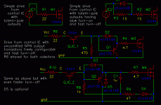
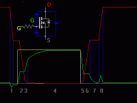
MOSFETS have high capacitances between G, D and S : 'Cgd', 'Cgs', 'Cds' as shown in the drawing. These capacitances couple to the gate everything happening in the drain
1 : Negative transiet coupled fron drain to gate throug Cgd
Before 2 : Some dead time. Then, gate happily charges until the thresold voltage is reached and the device starts to turn-on
2 : Gate charging, Vgs does not increase mostly because Vds is decreasing and this robs through Cgd most of the current supplied by the control circuit until Vds stops decreasing
3 : Rds-on is further reduced due to Vgs is increase
4 : The device is fully turned-on
5 : The gate is happily discharged until Rds increases enough to cause Vds to start rising [the device is no longer enough 'saturated' to be able to conduct all the current flowing through the inductive load]
6 : The rising slope on Vds robs again through Cgd most of the current provided by the control circuit. This phenomena provides a quasi-constant Vds slope that depends on the magnitude of turn-off gate current available
7 : The gate is further discharged, this process is slow since gate capacitance for low Vgs is higher and the resistor that discharges it is conected to ground [or worse : to one or two diode drops above ground]
8 : The device on the other side of the primary turns on causing a fast rise in Vds of this device. This fast rising slope is coupled to the gate through Cgd and tends to turn on the device again. This is called 'parasitistic turn-on' and must be avoided
tennisballg :
Your captures suggest you are suffering some degree of parasitistic turn-on. Look at the drain waveforms, they bounce up and down just after turn off of each device. Thiere shouln't be any bouncing at all
Try adding some RC damping to the primaries and look if bouncing is still there [It could be transformer resonance but it's less likely]
Then, try adding another 2uS of dead time and see if bouncing is stil there. If adding dead-time cures the bouncing then you should use higher dead time or speed-up MOSFET turn-off and reduce the impedance seen from the gate to ground to help reducing the positive spike coupled through Cdg and eliminate parasitistic turn-on
Attachments
Alright, I added an RC network, it took a little of the edge off the rising peak, but didn't help the falling peak. I tried shortening the duty cycle, but the spike didn't go away. I also lowered the resistance on my gates, still, nothing.
Then I tried lengthening the duty cycle. It seems to help with the falling edge, but there's still that beginning spike that I am not sure if I should be worried about. I think that by increasing the duty cycle what is happening is that the falling parasitic spike is merging into the "on time", therefore it has no way of parasitically switching back on, because it already is on...
420 ohm dead time resistor...this is where I was in the above photos
200 ohm...
100 ohm...
Then I tried lengthening the duty cycle. It seems to help with the falling edge, but there's still that beginning spike that I am not sure if I should be worried about. I think that by increasing the duty cycle what is happening is that the falling parasitic spike is merging into the "on time", therefore it has no way of parasitically switching back on, because it already is on...
420 ohm dead time resistor...this is where I was in the above photos
An externally hosted image should be here but it was not working when we last tested it.
200 ohm...
An externally hosted image should be here but it was not working when we last tested it.
100 ohm...
An externally hosted image should be here but it was not working when we last tested it.
I don't see signs of cross-conduction on these captures so the spike and bouncing may be simply due to transformer leakage inductance
There appears to be little or no parasitistic turn-on spike on the gate waveforms but it may be an artifact depending on where you are taking the ground of the probes
Try to connect the ground of the probes directly to the source and the tip direcly to the drain/gate and see if you get the same results [in case you are connecting them in other places]. Geting the same results definitely means no cross-conduction
Also try to damp the ringing on the primaries [one RC on each, 1/RC=F, use the maximum R and minimum C that work]. Then look for ringing on the secondaries [at diode turn-off] and try to damp it in the same way [you may need to zoom at the diode turn-off transient to see it]
I would like to see the turn-off with 420 ohm capture in more detail and with less ringing [the ringing doesn't allow to see clearly the waveform]
- Status
- This old topic is closed. If you want to reopen this topic, contact a moderator using the "Report Post" button.