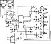
I have a problem with class D design. The design use HIP4080 from Intersil. The voltage is 75V, the triangle is about 250khz, the full bridge will be using 3 mosfets on each corner. The dead time is built by 330kohm//3.9nF. The highside charge pump is 220nF.
I tried first by putting IRF540 for the final mosfets. It doesn't work right, very distorted, and if I force it to work, it blows all the mosfets and the HIP.
In other thread, someone has mentioned that HIP has limitation on its output. Therefore, we have to calculate the output current of HIP, its working frequency, and the input capacitance of the mosfets.
I asked Intersil and they told me that I have to change the mosfets, with more suitable one (maybe less C input?).
If this is the answer, so the HIP4080 is not suitable for every design. It is very picky to the bridge mosfets.
Does anyone have experience with this HIP4080? Is there some trick so I can use any mosfets for bridge, can use any number of mosfet at any frequency (without concerning the input capacitance). What is to be modified with this HIP4080 circuit? The circuit is similiar to the standard HIP4080 APP note.
Some questions:
1) Did you make the PCB layout by yourself ? Layout is veeeeeeeery critical for switching amps ! Do you use any snubbers or the like in order to reduce overshoots ? Did you try without output filter fist and how did the rectangular look like on a CRO ?
2.) Do you stay within the HIP's max voltage limitations ?
3.) Do you stay within the HIP's dissipation limits ? This can be traded off against switching speed by the choice of gate series resistors. But I doubt that you will find any convenient full-bridge driver that can reasonably drive three 540s in parallel (i.e. 12 pieces in total) at 250 kHz.
Why do you need so many of them in parallel ? Do you know that there is a suffix N type of this mosfet with approximately half the on-resistance ?
Regards
Charles
1. No, the pcb is not by me. Snubbers, yes I use them. The circuit is similiar to the sch on the HIP APP note. The output is good rectangular
2. Yes, HIP is max 80V, I use 75V.
3. Dissipation? Dont know it. But if I touch the HIP, it is warm but normal.
I dont know about N suffix. Thanks for the info.
Why I use so much? Because I intended to use it for 1 ohm subwoofer load. Maybe this is where the problem originated. HIP is not designed for that much mosfets for each corner of the full bridge. How can we solve this?
Will playing with dead time will help? Or not? Or make the Charge pump capacitor bigger than 220nF? Or it will not help anything?
Currently I have too many parts burned. Too risky with guess work.
Even with 75 Volts you may still have overshoots going above 80 Volts even when the rectangular looks nice in a CRO (make sure that it's bandwidth is high enough !).
Does it die as soon as you connect a load or do you have to drive it hard ?
The following things might cause problems: Mosfet body-diode reverse recovery. Not enough dead-time. Too much dead-time. ........
What is the size of your gate series resistors ? If they are too small then there is too much dissipation in the driver IC. If they are too large you would have longer transistion time provoking increrased dissipation in your mosfets.
Glitches entering the comparator might cause increased stress for both the drivers and the mosfets.
If you want to use it only at subwoofer frequencies, you might use a switching frequency that is just above hearing. Dissipation is proportional to both , switching frequency AND total gate-charge.
Regards
Charles
Something else may be that you are experiencing power supply pumping which is blowing the chip
He is using a full bridge.
")
Noise can also be getting into a sensitive area which confuses the chip causing destruction.
Thats what I meant with glitches. I once had to learn this the hard way when I killed mosfet drivers for no apparent reason. They just don't like several on/off transistions while there should be just one taking place. Due to EMC reasons (being they capacitively, ohmically or inductively coupled, with the second and third more likely) this might even be load dependant. So make always sure that you have a good low-resistance/low-inductance ground-plane.
Regards
Charles
This is some story about this project. I have some boards. When I finished assembly one, I test it with low volume in subwoofer, it is OK. But when I crank up the volume, it become distorted. And if I dont shut it down, it blows all the mosfets+HIP.
Something is odd. When I finished assembly a brand new pcb, the dc offset is about 150mV (is this normal with HIP?There also some audible noise in the sub). But when I repair the same PCB and put all new mosfets and HIP, the dc offset is about 600mV. I cannot make it to 150mV like original, no matter I change the HIP or the mosfets. What is causing this raising DC offset? It gives me headache. Swapping component doesnt help, so it doesn't make any sense to me. What is changing after the power blow up (but I replaced with new components)
The Dead time is made by 330k//2n7. The APP stated that this resistor should not more than 250k, so I change it to 220k and remove the 2n7cap. It helps, but a little.
The gate of mosfets is made by 100ohm+IN4148, for every mosfet. I noticed some other manufacturer use only 1 100ohm//IN4148 for 3 mosfets at once (parrarel all the gates). What is the intention in doing this?
Just found out yesterday. I use FDP3672 instead of IRF540. It seems much better performance now. But not perfect yet. Maybe the FDP has lower capacitance. But the DC offset problem is still there.
What should I do if I still wanted to use IRF540? The FDP are hard to find here.
If this HIP still gives me headache, I wanted to built class D based on IRF schematic (like amp-man pointed). But the schematic is not clear, like it doesnt have triangle generator. Does anyone have complete schematic on this IRF class D and its complete documentation (like APP note, voltage checkpoints?)
- Status
- This old topic is closed. If you want to reopen this topic, contact a moderator using the "Report Post" button.
- Home
- Amplifiers
- Class D
- ClassD problem with HIP4080